Transistors are semiconductor triodes that have three outputs. Their main property is the ability to control high current at the outputs of the circuit using relatively low input signals.
For radio components that are used in modern complex electrical devices, field-effect transistors are used. Thanks to the properties of these elements, the current in the electrical circuits of printed circuit boards is turned on or off, or it is amplified.
What is a field effect transistor?
Field-effect transistors are three or four contact devices in which the current flowing to two contacts can be controlled by the electric field voltage of the third contact. on two contacts is regulated by the voltage of the electric field on the third. As a result, such transistors are called field-effect transistors.
Names of contacts located on the device and their functions:
- Sources – contacts with incoming electric current, which are located in section n;
- Drains are contacts with outgoing, processed current, which are located in section n;
- Gates are contacts located in section p, by changing the voltage at which the throughput of the device is adjusted.
Field effect transistors with np junctions are special types that allow you to control current. As a rule, they differ from simple ones in that current flows through them without crossing the section of p-n junctions, a section that is formed at the boundaries of these two zones. The dimensions of the p-n area are adjustable.
What it is
A field-effect transistor is a semiconductor type radio element. It is used to amplify the electrical signal. In any digital device, a circuit with a field-effect transistor plays the role of a key that controls the switching of the logical elements of the device. In this case, the use of PT is a very beneficial solution to the problem in terms of reducing the size of the device and board. This is due to the fact that the control circuit for radio components does not require very much power, which means that thousands and tens of thousands of transistors can be located on one chip.
Connection diagram for a field-effect transistor
The materials from which semiconductor elements and transistors are made are:
- indium phosphide;
- Gallium nitride;
- Gallium arsenide;
- Silicon carbide.
Graph of the saturation region of the electrotransistor
Important! Field-effect transistors are also called unipolar, since only one type of carrier is used when electric current flows through them.
Types of field effect transistors
A field-effect transistor with n-p junctions is divided into several classes depending on:
- From the type of conductor channels: n or r. Channels influence signs, polarities, control signals. They must be opposite in sign to the n-section.
- From the structure of the devices: diffuse, alloyed along p-n junctions, with Schottky gates, thin-film.
- Of the total number of contacts: can be three or four contacts. For four contact devices, the substrates are also gates.
- From the materials used: germanium, silicon, gallium arsenide.
In turn, the division of classes occurs depending on the principle of operation of the transistor:
- devices controlled by p-n junctions;
- devices with insulated gates or Schottky barriers.
Types of MOSFETs
Unipolar transistors are divided into p-channel or n-channel. They may have:
Own (built-in) channel. Without voltage, the channel is open. To close the channel, it is necessary to apply a current of a certain polarity.
Induced (inverse) channel. In the absence of applied electric current, it is closed. To open it, a voltage of the required polarity is applied. For n-channel transistors, the gate voltage is positive relative to the source. Its value must be greater than the threshold value set for a given transistor. For p-channel models, the gate voltage will be negative relative to the source and applied to the gate.
The principle of operation of a field-effect transistor
Speaking in simple words about how a field-effect transistor for dummies with control pn junctions works, it is worth noting: radio components consist of two sections: p-junctions and n-junctions. An electric current passes through section n. Section p is an overlapping zone, a kind of valve. If you apply a certain pressure to it, it will block the area and prevent the passage of current. Or, on the contrary, as the pressure decreases, the amount of current passing will increase. As a result of this pressure, the voltage increases at the contacts of the gates located on the river section.
Devices with control pn channel junctions are semiconductor wafers that have electrical conductivity of one of these types. The drain and source contacts are connected to the end sides of the plates, and the gate contacts are connected to the middle. The operating principle of the device is based on changing the spatial thickness of pn junctions. Since there are practically no mobile charge carriers in the blocking regions, their conductivity is zero. In semiconductor wafers, in areas of which the blocking layer is not affected, current-conducting channels are created. If a negative voltage is applied in relation to the source, a current is formed at the gate through which charge carriers flow.
Insulated gates are characterized by the placement of a thin layer of dielectric on them. This device operates on the principle of electric fields. It only takes a little electricity to destroy it. In this regard, in order to prevent static voltage, which can exceed 1000 V, it is necessary to create special housings for devices that minimize the effect of viral types of electricity.
How to solder field-effect transistors correctly and safely: 5 tips
I recommend that beginners pay close attention to this issue. Then you will not be disappointed with the work done.
Where is the ambush hidden or why is static dangerous for electronics?
In everyday life, we rarely feel static electricity, for example, when combing our hair with a plastic comb, getting out of the car after a trip, or in some other cases.
Usually, static causes minor troubles to our body that are simply annoying. But with semiconductors things are different.
MOSFETs have a very thin layer of insulation between the gate and the channel material. It forms a capacitive coupling between gate-source and gate-drain. Moreover, the dielectric itself creates this effect, working as a capacitance.
We know that any capacitor is manufactured to operate at a certain voltage. If it is exceeded, an insulation breakdown occurs. Ten volts are usually enough to damage the oxide film of the field grass, and sometimes less.
Now I’m showing with photographs what dangers we can create for transistors with our own hands if we don’t follow the rules for soldering them.
I took my favorite Moment transformer soldering iron, plugged its power cord into the outlet, but did not press the power button. I placed one end of the multimeter wire through an alligator clip onto the sting, and the other just leaned it against my finger. Set the AC voltmeter mode.
The device shows 28 volts. This is the kind of interference that is created even when the transformer is de-energized.
I continue the experiment. I left the black probe in the same place, and leaned the red one against the dielectric surface of the stool, where all the instruments are located.
Almost 6.4 volts. When I separated the red probe with air space, the reading became 8 volts.
But these are completely random measurements, the results of which depend on many factors, which means: the voltage can be significantly more or less.
We may not even feel this static, but its random discharge can burn out the thin semiconductor junction of the crystal.
To prevent this, it is important to follow the mandatory recommendations.
How to avoid hidden dangers and work safely with a soldering iron: 5 recommendations
Tip #1: Bypassing the leads
Damage to semiconductor junctions during storage and operation can be prevented by keeping microcircuits, transistors, and integrated electronics products in a layer of foil.
A similar result, in particular, is obtained if you wrap the contacts of their terminals with thin copper wire without insulation.
Tip #2: removing static from operating equipment
It is best to work with a professional soldering station with a grounded tip. If it is not there, then ground the soldering iron tip and the circuit board with separate conductors. Shunt the transistor leads with a thin wire, which will be removed after soldering.
A grounding bracelet on your hand or other part of the body allows you to remove the dangerous potential of static from tweezers and the tool you will be working with. Its 1 MΩ resistance eliminates the possibility of dangerous static discharge.
Tip No. 3: preparing the workplace
The dry air of northern latitudes, especially in winter, contributes to the accumulation of static on surrounding objects. Humidifiers and air washes successfully combat this phenomenon.
An antistatic mat immediately and reliably removes static potentials and the effects of electrical noise from the environment.
Tip #4: professional mixtures
A special flux of the FluxOff brand not only perfectly washes away rosin and traces of corrosion, but actually removes static. They just need to wet the board.
Tip #5: Quick soldering
Choose the minimum required soldering iron power, but work quickly with it. Experienced repairmen manage to heat up the tip, take solder with it, turn off the power to the soldering iron and then solder the part in place.
Some modern microcircuits and transistors are protected against static, but this does not eliminate the need to follow the rules of safe soldering with all other products.
What is a field effect transistor used for?
When considering the operation of complex types of electrical engineering, it is worth considering the operation of such an important component of an integrated circuit as a field-effect transistor. The main task of using this element lies in five key areas, and therefore the transistor is used for:
- High frequency amplification.
- Low frequency boost.
- Modulations.
- DC amplification.
- Key devices (switches).
As a simple example, the operation of a transistor switch can be represented as a microphone and a light bulb in one arrangement. Thanks to the microphone, sound vibrations are captured, which affects the appearance of electric current flowing to the area of the locked device. The presence of current affects the switching on of the device and the switching on of the electrical circuit to which the light bulbs are connected. The latter light up after the microphone has picked up the sound, but they burn due to power sources not connected to the microphone and more powerful.
Modulation is used to control information signals. The signals control the oscillation frequencies. Modulation is used for high-quality audio radio signals, for transmitting audio frequencies to television broadcasts, for broadcasting color images and television signals with high quality. Modulation is used everywhere where it is necessary to work with high-quality materials.
As amplifiers, field-effect transistors work in a simplified form according to the following principle: graphically, any signals, in particular audio, can be represented as a broken line, where its length is the time interval, and the height of the breaks is the audio frequency. To amplify the sound, a powerful voltage flow is supplied to the radio component, acquiring the desired frequency, but with a higher value, due to the supply of weak signals to the control contacts. In other words, thanks to the device, a proportional redrawing of the original line occurs, but with a higher peak value.
The difference between unipolar transistors and bipolar ones
The MOSFET is controlled by an electric field, which is created by a voltage applied to the gate relative to the source. The polarity of the applied voltage is determined by the type of transistor channel (p or n). Unlike unipolar bipolar transistors, they are controlled by electric current. The current in all types of these semiconductors is formed by two types of charges - electrons and holes.
Field-effect (unipolar) transistors, unlike bipolar ones, have lower intrinsic noise in the low-frequency range. This property ensures their effective operation in sound amplification devices. MOSFETs are used in low-frequency amplifier microcircuits in car players.
How to use a field-effect transistor for dummies
The first devices that entered the market for sale, and in which field-effect transistors with control pn junctions were used, were hearing aids. Their invention took place back in the fifties of the 20th century. On a larger scale they were used as elements for telephone exchanges.
Nowadays, the use of such devices can be seen in many types of electrical engineering. Having small sizes and a large list of characteristics, field-effect transistors are found in kitchen appliances (toasters, kettles, microwaves), in computer, audio and video equipment and other electrical appliances. They are used for fire safety alarm systems.
In industrial enterprises, transistor equipment is used to regulate power on machine tools. In the transport sector, they are installed in trains and locomotives, and in fuel injection systems for personal cars. In the housing and communal services sector, transistors make it possible to monitor dispatching and street lighting control systems.
Also, the most popular area in which transistors are used is the manufacture of components used in processors. The design of each processor includes multiple miniature radio components, which, when the frequency increases by more than 1.5 GHz, require increased energy consumption. In connection with these, processor technology developers decided to create multi-core equipment rather than increase the clock frequency.
How does a bipolar transistor work? Instructions for dummies
The operation of bipolar transistors is based on the properties of semiconductors and their combinations. To understand the principle of operation of triodes, let's understand the behavior of semiconductors in electrical circuits.
Semiconductors.
Some crystals, such as silicon, germanium, etc., are dielectrics. But they have one feature - if you add certain impurities, they become conductors with special properties.
Some additives (donors) lead to the appearance of free electrons, while others (acceptors) create “holes”.
If, for example, silicon is doped with phosphorus (donor), we obtain a semiconductor with an excess of electrons (n-Si structure). By adding boron (an acceptor), the doped silicon will become a hole-conducting semiconductor (p-Si), that is, its structure will be dominated by positively charged ions.
One-way conduction.
Let's conduct a thought experiment: connect two different types of semiconductors to a power source and supply current to our design. Something unexpected will happen. If you connect the negative wire to an n-type crystal, the circuit will be completed. However, when we reverse the polarity, there will be no electricity in the circuit. Why is this happening?
As a result of connecting crystals with different types of conductivity, a region with a pn junction is formed between them. Some electrons (charge carriers) from an n-type crystal will flow into a crystal with hole conductivity and recombine holes in the contact zone.
As a result, uncompensated charges arise: in the n-type region - from negative ions, and in the p-type region from positive ions. The potential difference reaches values from 0.3 to 0.6 V.
The relationship between voltage and impurity concentration can be expressed by the formula:
φ= VT * ln (Nn * Np)/n2i, where
VT is the value of the thermodynamic stress, Nn and Np are the concentration of electrons and holes, respectively, and ni denotes the intrinsic concentration.
When connecting a plus to a p-conductor and a minus to an n-type semiconductor, the electric charges will overcome the barrier, since their movement will be directed against the electric field inside the pn junction. In this case, the transition is open. But if the poles are reversed, the transition will be closed. Hence the conclusion: the pn junction forms one-way conductivity. This property is used in the design of diodes.
From diode to transistor.
Let's complicate the experiment. Let's add another layer between two semiconductors with the same structures. For example, between p-type silicon wafers we insert a conductivity layer (n-Si). It is not difficult to guess what will happen in the contact zones. By analogy with the process described above, regions with pn junctions are formed, which will block the movement of electrical charges between the emitter and collector, regardless of the polarity of the current.
The most interesting thing will happen when we apply a slight voltage to the layer (base). In our case, we will apply a current with a negative sign. As in the case of a diode, an emitter-base circuit is formed through which current will flow. At the same time, the layer will begin to become saturated with holes, which will lead to hole conduction between the emitter and collector.
Look at Figure 7. It shows that positive ions have filled the entire space of our conditional structure and now nothing interferes with the conduction of current. We have obtained a visual model of a bipolar transistor with a pnp structure.
Rice. 7. Principle of operation of the triode
When the base is de-energized, the transistor very quickly returns to its original state and the collector junction closes.
The device can also operate in amplification mode.
The collector current is directly proportional to the base current: Iк = ß*IB , where ß is the current gain, IB is the base current.
If you change the value of the control current, the intensity of hole formation on the base will change, which will entail a proportional change in the amplitude of the output voltage, while maintaining the signal frequency. This principle is used to amplify signals.
By applying weak pulses to the base, at the output we get the same amplification frequency, but with a much larger amplitude (set by the voltage applied to the collector-emitter circuit).
NPN transistors work in a similar way. Only the polarity of the voltages changes. Devices with NPN structure have direct conductivity. PNP type transistors have reverse conductivity.
It remains to add that the semiconductor crystal reacts in a similar way to the ultraviolet spectrum of light. By turning the photon flow on and off, or adjusting its intensity, you can control the operation of a triode or change the resistance of a semiconductor resistor.
Bipolar transistor connection circuits
Circuit designers use the following connection schemes: with a common base, common emitter electrodes, and connection with a common collector (Fig. 8).
Rice. 8. Connection diagrams for bipolar transistors
Amplifiers with a common base are characterized by:
- low input impedance, which does not exceed 100 Ohms;
- good temperature properties and frequency characteristics of the triode;
- high permissible voltage;
- two different power sources are required.
Common emitter circuits have:
- high current and voltage gain;
- low power gain;
- inversion of the output voltage relative to the input.
With this connection, one power source is sufficient.
The connection diagram based on the “common collector” principle provides:
- high input and low output resistance;
- low voltage gain factor (< 1).
Advantages and disadvantages of field-effect transistors
The use of field-effect transistors, due to their universal characteristics, made it possible to bypass other types of transistors. They are widely applied to integrated circuit as switch.
Advantages:
- cascades of parts consume a small amount of energy;
- amplification indicators exceed the values of other similar devices;
- high noise immunity is achieved due to the fact that there is no current in the gate;
- have a higher turn-on and turn-off speed and operate at frequencies inaccessible to other transistors.
Flaws:
- less resistant to high temperatures, which lead to destruction;
- at frequencies above 1.5 GHz, the amount of energy consumed increases rapidly;
- sensitive to static types of electricity.
Thanks to the characteristics possessed by semiconductor materials, taken as the basis for a field-effect transistor, they allow the device to be used in household and industrial applications. Various household appliances that are used by modern people are equipped with field-effect transistors.
What is a transistor?
In its modern meaning, a transistor is a semiconductor radio element designed to change the parameters of an electric current and control it. A conventional semiconductor triode has three terminals: a base, which receives control signals, an emitter, and a collector. There are also high power composite transistors.
The size scale of semiconductor devices is striking - from several nanometers (unpackaged elements used in microcircuits) to centimeters in diameter for high-power transistors intended for power plants and industrial equipment. Reverse voltages of industrial triodes can reach up to 1000 V.
Device
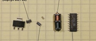
Structurally, the triode consists of semiconductor layers enclosed in a housing. Semiconductors are materials based on silicon, germanium, gallium arsenide and other chemical elements. Today, research is being conducted to prepare certain types of polymers, and even carbon nanotubes, for the role of semiconductor materials. Apparently in the near future we will learn about new properties of graphene field-effect transistors.
Previously, semiconductor crystals were located in metal cases in the form of caps with three legs. This design was typical for point-point transistors.
Today, the designs of most flat, including silicon semiconductor devices are made on the basis of a single crystal doped in certain parts. They are pressed into plastic, metal-glass or metal-ceramic cases. Some of them have protruding metal plates for heat dissipation, which are attached to the radiators.
The electrodes of modern transistors are arranged in one row. This arrangement of the legs is convenient for automatic board assembly. The terminals are not marked on the housings. The type of electrode is determined from reference books or by measurements.
For transistors, semiconductor crystals with different structures, such as pnp or npn, are used. They differ in the polarity of the voltage on the electrodes.
Schematically, the structure of a transistor can be represented as two semiconductor diodes separated by an additional layer. (See Figure 1). It is the presence of this layer that allows you to control the conductivity of the semiconductor triode.
Rice. 1. Structure of transistors
Figure 1 schematically shows the structure of bipolar triodes. There is also a class of field-effect transistors, which will be discussed below.
Basic operating principle
At rest, no current flows between the collector and emitter of a bipolar triode. Electric current is prevented by the resistance of the emitter junction, which arises as a result of the interaction of the layers. To turn on the transistor, you need to apply a small voltage to its base.
Figure 2 shows a diagram explaining the working principle of a triode.
Rice. 2. Operating principle
By controlling the base currents, you can turn the device on and off. If an analog signal is applied to the base, it will change the amplitude of the output currents. In this case, the output signal will exactly repeat the oscillation frequency at the base electrode. In other words, the electrical signal received at the input will be amplified.
Thus, semiconductor triodes can operate in electronic switch mode or in input signal amplification mode.
The operation of the device in electronic key mode can be understood from Figure 3.
Rice. 3. Triode in switch mode
Designation on diagrams
The generally accepted designation is “VT” or “Q” , followed by a positional index. For example, VT 3. On earlier diagrams you can find outdated designations: “T”, “PP” or “PT”. The transistor is depicted as symbolic lines indicating the corresponding electrodes, circled or not. The direction of current in the emitter is indicated by an arrow.
Figure 4 shows a ULF circuit in which transistors are designated in a new way, and Figure 5 shows schematic images of different types of field-effect transistors.
Rice. 4. Example of a ULF circuit using triodes