This is an amplifier that not only has two low-power channels, but also has a high efficiency rate with a low current-consumption ratio.
This device provides exceptional value for sensitive “systems” with characteristics such as low offset (300 µV typical), common mode range to ground, and high differential input pressure capability.
The op-amp simplifies circuit design with the following advanced features: unity gain stability, lower offset voltage of 3 mV (maximum at room temperature), and a “much lower” quiescent current of 300 µA. Serious electrostatic discharge (2 kV, HBM) and built-in EMI and RF filters allow the device to be used in the harshest and most environmentally demanding “grids”.
It is worth saying that this device is capable of functioning even in unipolar power supply structures (4-30 Volt range), this is due to the presence of a dual internal unit that protects the entire system from short-term short circuits.
Purpose
Why do you need a comparator and how to use it without an amplifier?
In most cases, this device is used in simple computer circuits where it is necessary to compare incoming voltage signals. This can be a charger for a laptop or phone, a scale (mass meter), an AVR mains voltage sensor, a timer (composer type lm 358, microcontroller, etc. It is also used by various integrated circuits to control input pulses, providing communication between the signal source and its destination center. The most popular example is the comparator trigger (regulator) Shimmer. It operates in multi-channel mode, accordingly, it can compare a large number of signals. In particular, this trigger is used to restore a digital signal that distorts the connection depending on voltage level and distance of the power source.
This is an analogue of a standard comparator, just with more advanced functionality, which provides measurement of several incoming signals.
There is also a roughness comparator. This is a device that helps to visually determine the condition of a surface that has already been treated. The use of this device is justified by the need to determine the tolerances of previously processed surfaces.
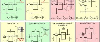
Popular circuits for lm358
There are various devices assembled on the LM358 N that perform specific functions. In this case, these can be all kinds of amplifiers, both UMZCH and in intermediate circuits for measuring various signals, an LM358 thermocouple amplifier, comparing circuits, analog-to-digital converters, etc.
Non-inverting amplifier and voltage reference
These are the most popular types of wiring diagrams used in many devices to perform various functions. In a non-inverting amplifier circuit, the output voltage will be equal to the product of the input voltage and the proportional gain formed by the ratio of two resistances included in the inverting circuit.
The voltage reference circuit is highly popular due to its high practical performance and stability in various modes. The circuit perfectly maintains the required output voltage level. It has been used to build reliable and high-quality power supplies, analog signal converters, and in devices for measuring various physical quantities.
Sine Wave Generator
One of the highest quality sine wave generator circuits is the Wien bridge device . With the correct selection of components, the generator produces pulses in a wide range of frequencies with high stability. Also, the LM 358 chip is often used to implement a rectangular pulse generator of various duty cycles and durations. At the same time, the signal is stable and high quality.
Amplifier
The main applications of the LM358 chip are amplifiers and various amplification equipment. This is ensured due to the inclusion features and selection of other components. This circuit is used, for example, to implement a thermocouple amplifier.
Thermocouple amplifier on LM358
Very often in the life of a radio amateur it is necessary to monitor the temperature of some devices. For example, on a soldering iron tip . You can’t do this with an ordinary thermometer, especially when you need to create an automatic control circuit. For this, you can use the LM 358 op-amp. This microcircuit has a low thermal zero drift, and therefore is classified as high-precision. Therefore, it is actively used by many developers for the manufacture of soldering stations and other devices.
Read also: How to properly sharpen a circular saw
The circuit allows you to measure temperature in a wide range from 0 to 1000 o C with a fairly high accuracy of up to 0.02 o C. The thermocouple is made of a nickel-based alloy: chromal, alumel. The second type of metal has a lighter color and is less susceptible to magnetization; chromal is darker and magnetizes better. Features of the circuit include the presence of a silicon diode, which should be placed as close as possible to the thermocouple. When heated, the chromal-alumel thermoelectric pair becomes an additional source of emf, which can make significant adjustments to the main measurements.
Simple current regulator circuit
The circuit includes a silicon diode . The transition voltage from it is used as a source of a reference signal, supplied through a limiting resistor to the non-inverting input of the microcircuit. To adjust the stabilization current of the circuit, an additional resistor is used, connected to the negative terminal of the power supply, to the non-inverting input of the MS.
The circuit consists of several components:
- A resistor supporting the op-amp with a negative terminal and a resistance of 0.8 Ohms.
- A resistive voltage divider consisting of 3 resistances with a diode serving as a reference voltage source.
An 82 kOhm resistor is connected to the negative of the source and the positive input of the MS. The reference voltage is formed by a divider consisting of a 2.4 kOhm resistor and a directly connected diode. After which the current is limited by a 380 kOhm resistor. The op-amp controls a bipolar transistor, the emitter of which is connected directly to the inverting input of the MS, forming a negative deep connection. Resistor R 1 acts as a measuring shunt. The reference voltage is formed using a divider consisting of a diode VD 1 and a resistor R 4.
In the presented circuit, provided that resistor R2 with a resistance of 82 kOhm is used, the stabilization current in the load is 74 mA at an input voltage of 5V. And when the input voltage increases to 15V, the current increases to 81mA. Thus, when the voltage changes by a factor of 3, the current changes by no more than 10%.
Description of the LM358 chip
Confirmation of the high popularity of the microcircuit is its performance characteristics, which allow the creation of many different devices. The main indicative characteristics of the component include the following.
Acceptable operating parameters: the microcircuit provides single and bipolar power supply, a wide range of supply voltages from 3 to 32 V, an acceptable slew rate of the output signal equal to only 0.6 V/μs. Also, the chip consumes only 0.7 mA, and the offset voltage is only 0.2 mV.
In what packages are microcircuits produced?
The housing can be either DIP8 - designation LM358N, or SO8 - LM358D. The first is intended for the implementation of volumetric installation, the second - for surface installation. The characteristics of the element do not depend on the type of housing - they are always the same. But there are many analogues of the microcircuit, whose parameters are slightly different. There are always pros and cons. Typically, if an element has a large range of operating voltages, for example, some other characteristic suffers.
There is also a metal-ceramic case, but such microcircuits are used if the device will be used in difficult conditions. In amateur radio practice, it is most convenient to use microcircuits in surface-mount packages. They solder very well, which is important when working. After all, it turns out to be much more convenient to work with elements whose legs are longer.
Main Parameters of LM358
The sensor has several key parameters at once. These are the ones that will be discussed in this section.
Let's start, perhaps, with “limited gain,” which is denoted as follows: [gopen.]. This is a certain indicator that demonstrates how many times the “op-amp” has increased the operating frequency of the initial signal.
Now let's look at the second most important element - [vout.] - the voltage at the output. [vout.] cannot be infinite, because it is precisely this that ensures equality in transition phases.
And finally, [rres.] is the resulting resistance, which shows the maximum “value” of the resistors used in the circuit.
Characteristics table
| Parameter | LM358, LM358N |
| Power, volts | 3-32V |
| Bipolar nutrition | ±1.5V to ±16V |
| Current consumption | 0.7mA |
| Input offset voltage | 3mV |
| Input compensation offset current | 2nA |
| Input current offset | 20nA |
| Output slew rate | 0.3 V/ms |
| Output current | 30 - 40mA |
| Maximum frequency | 0.7 to 1.1 MHz |
| Differential Gain | 100dB |
| Working temperature | 0° to 70° |
Microcircuits from different manufacturers may have different parameters, but everything is within normal limits. The only thing that can differ greatly is the maximum frequency: for some it is 0.7 MHz, for others it is up to 1.1 MHz. There are a lot of options for using ICs; there are about 20 of them in the documentation alone. Radio amateurs have expanded this number to more than 70 schemes.
We recommend reading: Zener diode characteristics, marking, principle of operation
Typical functionality from the datasheet in Russian:
- comparators;
- active RC filters;
- LED driver;
- DC summing amplifier;
- pulse and pulsation generator;
- low voltage peak voltage detector;
- bandpass active filter;
- for amplification from a photodiode;
- inverting and non-inverting amplifier;
- balanced amplifier;
- current stabilizer;
- AC inverting amplifier;
- DC differential amplifier;
- bridge current amplifier.
Designation and technical specifications
A comparator is a device that compares two different voltages and currents, produces a final power signal indicating the greater of them, while simultaneously calculating the ratio. It has two analog input terminals with positive and negative signals and one binary digital output, just like an ADC. A special indicator is used to display the signal.
The UGO display of the comparator looks like this:
Photo – UGO comparator
Initially, only the integrated voltage comparator (MAX 961ESA, PIC 16f628a) was used, which is known as high-speed. It requires a certain differential voltage within a certain range, which is significantly lower than the mains voltage. These devices do not accept any other external signals that are outside the mains voltage range.
Nowadays, an analog digital comparator (Attiny/ Atmega 2313), which has a transistor input, is much more often used. Its input signal potential is in the range of less than 0.3 Volts and does not rise higher. The device can also be of an ultra-fast type (stereo comparator), due to which the input signal is less than the designated range, for example, 0.2 Volts. Typically, the usable range is limited only by the specific input voltage.
Photo – Comparator
In addition to a simple device, there is also a video spectral comparator based on an op-amp (operational amplifier). This is a device that has a very finely balanced difference between the input and high signal impedance. Due to this characteristic, the operational comparator is used in low-conductivity circuits with low voltage.
Photo - comparator circuit
In theory, a frequency op-amp operates in an open-loop configuration (no negative feedback) and can be used as a low-performance comparator. But at the same time, the non-inverting input (+ V) is at a higher voltage than the inverting input (V-). The high gain output from the op amp causes a low voltage output at the input to the device.
When the non-inverting input falls below the inverting input, the output signal saturates at a negative supply level, then it can still conduct pulses. The output voltage of the op amp is limited only by the supply voltage. The circuit diagram of the op-amp operates in linear mode with negative feedback, using a balanced split power supply (powered by ± VS). Many devices that work with a comparator also tend to record the received data using video, photo or documentary recording. These electronic principles do not work in systems that use open loops and low conductivity components.
Photo - a simple comparator
But the comparator amplifier has several significant disadvantages :
- Op-amps are designed to operate in linear mode with negative feedback. But at the same time, the op-amp has a longer recovery mode;
- Almost all op amps have an internal compensation capacitor that limits the slew rate of the output voltage for high frequency signals. Based on this, this circuit slightly delays the impulse;
- The comparator has no internal hysteresis.
Due to these disadvantages, a comparator for controlling various circuits is, in most cases, used without an amplifier, with the exception of an oscillator.
The comparator is designed for manufacturing processes with limited output voltage that interfaces easily with digital logic. Therefore, it is often used in various thermal devices (thermostat, temperature switch). It is also used to compare signals and resistances of devices such as timers, stabilizers and other circuitry.
Photo – analog comparator
Video: Comparators
Application
- pulse and pulsation generator (devices of the “flashing beacon” type);
- power supplies and chargers;
- split systems for indoor and outdoor use;
- motherboards;
- Appliances;
- balanced amplifier;
- bridge current amplifier;
- engine control circuits;
- uninterruptible power supplies;
- refrigeration units, dishwashers and washing machines;
- various types of inverters;
- controllers and more.
Manufacturers, as a rule, indicate the areas of application of the microcircuit in technical descriptions.
Connection diagrams
Below are some simple lm358 connection diagrams that may be useful to you. These are all previews, so be sure to test everything before implementing it in production.
Circuit in a powerful non-inverting amplifier.
Voltage - current converter.
Circuit with differential amplifier.
Non-inverting medium power amplifier.
Non-inverting amplifier circuit
Description of the scheme:
- A signal is sent to the positive input.
- Two fixed resistors R2 and R1 connected in series are connected to the output of the operational amplifier.
- The second resistor is connected to the common wire.
- The connection point of the resistors is connected to the negative input.
To calculate the gain, you need to use a simple formula: k=1+R2/R1.
If there is data on the value of resistances and input voltage, then it is easy to calculate the output: U(out)=U(in)*(1+R2/R1). When using the LM358 microcircuit and resistors R1=10 kOhm and R2=1 MOhm, the gain will be equal to 101.
Circuit of a powerful non-inverting amplifier
Elements that are used in the design of a non-inverting amplifier and their parameters:
- The chip used is LM358.
- Resistance value R1=910 kOm.
- R2=100 kOm.
- R3=91 kOm.
To amplify the signal, a semiconductor bipolar transistor VT1 is used.
In terms of voltage, the gain, provided such elements are used, is equal to 10. To calculate the gain in the general case, you need to use the following formula: k=1+R1/R2. To calculate the current coefficient of the entire circuit, you need to know the corresponding parameter of the transistor used.
Voltage-to-current converter circuit
The circuit is shown in the figure and is somewhat similar to the one described in the design of a non-inverting amplifier. But here a bipolar transistor is added. The output current is directly proportional to the voltage at the input of the operational amplifier.
And at the same time, the current strength is inversely proportional to the resistance of resistor R1. If we describe this in formulas, it looks like this:
I=U(in)/R.
With a resistance value of R1 = 1 Om, for every 1V of voltage applied to the input, there will be 1A of current at the output. The LM358 connection circuit in voltage-to-current converter mode is used by radio amateurs to design chargers.
Current-voltage converter circuit
With this simple design, the LM358 op amp can convert low current to high voltage. This can be described with the following formula:
U(out)=I*R1.
If a resistor with a resistance of 1 MΩ is used in the design, and a current with a value of 1 μA flows through the circuit, then a voltage with a value of 1 V will appear at the output of the element.
We recommend reading: DIY generator voltage regulator relay: diagram
Simple differential amplifier circuit
This design is widely used in devices that measure voltage from sources with high resistance. A special feature that must be taken into account is that the resistance ratios R1/R2 and R4/R3 must be equal. Then the output voltage will have the following value:
U(out)=(1+R4/R3)*(Uin1-Uin2).
In this case, the gain can be calculated using the formula k=(1+R4/R3). If the resistance of all resistors is 100 kOhm, the coefficient will be equal to 2.
Current monitor circuit
Another circuit that allows you to measure the current value in the supply wire. It consists of a shunt resistor R1, an operational amplifier LM358, an NPN transistor and two resistors. Element characteristics:
- chip DA1 – LM358;
- resistor resistance R=0.1 Ohm;
- resistance value R2=100 Ohm;
- R3=1 kOhm.
The op-amp supply voltage must be at least 2 V higher than that of the load. This is a prerequisite for the functioning of the scheme.
Voltage to frequency converter circuit
This device will be required when there is a need to calculate the period or frequency of a signal.
The circuit is used as an analog-to-digital converter. Parameters of elements used in the design:
- DA1 – LM358;
- C1 – 0.047 µF;
- R1=R6=100 kOhm;
- R2=50 kOhm;
- R3=R4=R5=51 kOhm;
- R6=100 kOhm;
- R7=10 kOhm.
These are all designs that can be built using an op-amp. But the scope of the LM358 is not limited to this; there are a large number of much more complex circuits that allow you to implement various possibilities.
LM358 switching circuit: differential amplifier with adjustable gain
It is worth noting that the previous circuit does not allow you to adjust the gain, since it requires simultaneous changes in two resistors. If you need to be able to adjust the gain in a differential amplifier, you can use a circuit with three operational amplifiers. In this circuit, the gain is adjusted by adjusting resistor R2. For this circuit, it is necessary to meet the conditions for equality of resistor resistance values: R1 = R3 and R4 = R5 = R6 = R7. Then the gain will be equal to: (1+2*R1/R2). Uout = (1+2*R1/R2)(Uin1 – Uin2).
Working conditions
VCC = ±15 V, TA = 25°C
| Parameter | Conditions | TYP | Unit change | |
| S.R. | Slew rate at unity gain | RL = 1 MΩ, CL = 30 pF, VI = ±10 V (see Fig. 3) | 0.3 | V/μs |
| B1 | Bandwidth at unity gain | RL = 1 MΩ, CL = 20 pF (see Fig. 3) | 0.7 | MHz |
| Vn | Equivalent noise voltage referred to input | RS = 100 Ohm, VI = 0 V, f = 1 kHz (see Fig. 4) | 40 | nV/vHz |
Unity gain amplifier
Circuit for checking noise
Comparator with and without hysteresis
The initial data for the calculation are presented in the tables.
Table. Initial data for calculating the comparator
| Entrance | Exit | Nutrition | ||||
| ViMin | ViMax | VoMin | VoMax | Vcc | Vee | Vref |
| 0 V | 5 V | 0 V | 5 V | 5 V | 0 V | 5 V |
Table. Thresholds
| Lower switching threshold VL | Upper switching threshold VH | VH–VL |
| 2.3 V | 2.7 V | 0.4 V |
Description of the scheme
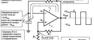
Comparators are used to compare two input signals and generate an output signal depending on which of the input signals is larger (Figure 84). Noise or bounce on the input signals can cause the comparator to switch multiple times. To combat such switchings, hysteresis is used, which sets the upper and lower switching limits.
Rice. Comparator circuits with hysteresis (left) and without hysteresis (right)
We recommend that you pay attention to:
- a comparator with minimal intrinsic current consumption should be used;
- the accuracy of setting the hysteresis threshold values is determined by the accuracy of the resistor values;
- The response delay is determined by the parameters of the comparator used.
We recommend reading: Thyristors: principle of operation, testing and characteristics
Principle of operation
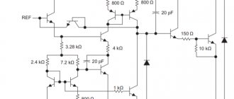
To demonstrate how a high-speed comparator with hysteresis works, you need to take a circuit with two outputs.
The connection diagram, from which you can understand the principle of operation of the comparator, is shown above. Using an analog signal at the + input, called "non-inverting", and the output, called "inverting", the device uses two similar signals of opposite polarity. However, if the analog input is greater than the analog output, then the output will be “1” and this will turn on the open collector of transistor Q8 on the LM339 equivalent circuit to be turned on. But, if the input is at a negative level, then the signal will be equal to “0”, which is why the collector will be closed.
Almost always, a two-threshold or phase comparator (for example, on transistors, without an amplifier) acts on the inputs in logic circuits, and accordingly, operates at the level of a certain power network. This is a kind of transition element between analog and digital signals. This principle of operation makes it possible not to specify the certainty or uncertainty of signal outputs, since the comparator always has some capture of the hysteresis loop (regardless of its level) or a final gain.
Procedure for calculating a comparator with hysteresis
- Select the value of resistor R1 = 100 kOhm. The threshold voltage values were determined in the source data table: VL = 2.3 V, VH = 2.7 V.
- Let's calculate R2 using formula 1:
- Let's calculate R3 using formula 2:
- We check the obtained hysteresis value according to formula 3:
How to calculate a comparator without hysteresis
- We select the threshold value Vth = 2.5 V.
- We select the value of resistor R4 = 100 kOhm.
- We calculate R5 using formula 4:
Circuit Simulation
Timing diagrams of the circuit operation are presented in Figures 1 and 2.
Rice. 1. Timing diagrams of the circuit operation: noise is present only in the initial short time interval 0...120 μs
Rice. 2. Enlarged voltage oscillogram: interval 40…110 µs
LM358 switching circuit: differential amplifier with adjustable gain
It is worth noting that the previous circuit does not allow you to adjust the gain, since it requires simultaneous changes in two resistors. If you need to be able to adjust the gain in a differential amplifier, you can use a circuit with three operational amplifiers. In this circuit, the gain is adjusted by adjusting resistor R2. For this circuit, it is necessary to meet the conditions for equality of resistor resistance values: R1 = R3 and R4 = R5 = R6 = R7. Then the gain will be equal to: (1+2*R1/R2). Uout = (1+2*R1/R2)(Uin1 – Uin2).