Field semiconductors
The MOSFET technology semiconductors used in inverters are field-effect power transistors with an insulated gate. The semiconductor is controlled by voltage, unlike bipolar transistors, which are controlled by current. The key channel has a high conductivity of 1 mOhm. When closed, they have a huge input impedance.
Initially, field-field semiconductors were and are still used as switches. In switching power supply circuits, field switches with an induced gate are used. In this design, at zero gate-source voltage, the channel is closed.
To open the key, a potential of a certain polarity must be applied. No power sources are required to operate the key. These semiconductors are often used in power supplies and inverters.
IGBT and MOSFET input impedance
IGBT is a voltage controlled bipolar device with high input impedance and high capacitance bipolar transistor. They can be easily controlled compared to current controlled devices in high precision applications. MOSFETs require almost no input current to drive load current, which makes them more resistive at the gate terminal due to the insulating layer between the gate and channel. The layer is made of silicon oxide, which is one of the best insulators used. It effectively blocks applied voltage except for small leakage current.
Bipolar device
IGBT is an insulated gate bipolar transistor used in inverter. In fact, it consists of two transistors on one substrate. The bipolar device forms a power channel, and the field one is a control channel.
The connection of two types of semiconductors allows you to combine the advantages of field and bipolar devices in one device. The combined device can, like a bipolar device, operate with high potentials; the channel conductivity is inversely proportional to the current, and not its square, as in a field-effect transistor.
In this case, the IGBT transistor has economical field device control. The power electrodes are called as in a bipolar device, and the control electrode is called a gate, as in a MOS device.
IGBT transistors for welding inverters and power drives, where they have to operate at high voltages, began to be used as soon as the technology for their production was debugged. They reduced the size, increased the performance and power of inverters. Sometimes they even replace thyristors.
In an IGBT inverter, to ensure the operation of powerful switches, drivers are used - microcircuits that amplify the control signal and accelerate fast charging of the gate.
Some models of IGBT transistors operate with voltages from 100 V to 10 kV and currents from 20 to 1200 A. Therefore, they are more often used in power electric drives and welding machines.
Field-effect transistors are more often used in pulsed sources and single-phase welding inverters. With current parameters of 400-500 V and 30-40 A, they have the best performance characteristics. But since IGBT devices can be used in more severe conditions, they are increasingly used in welding inverters.
general information
Transistors - what are they? Surely everyone who has ever encountered the repair or banal disassembly of radio electronics has heard this term. In simple terms, a transistor is an electronic part with terminals made of semiconductor material. The main function of a transistor is to amplify or generate electrical signals coming from outside. Switching is also performed using transistors.
At the moment, transistors are found in any electronic device and are one of the most important components. In the middle of the last century, several scientists received the Nobel Prize for the invention of the transistor. And since then, this small device has radically changed the world of electronics.
Transistors are very small and compact. They are economical and inexpensive to produce. Despite its modest size, the transistor is resistant to mechanical stress and durable. Transistors are also able to operate properly at low voltages and high currents. It was thanks to these advantages that by the end of the 20th century, transistors became an integral part of every electronic device. Including inverter welding machines.
Welding Application
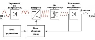
A simple welding inverter is a switching power source. In a single-phase inverter power supply, alternating current with a voltage of 220 V and a frequency of 50 or 60 Hz is rectified using powerful diodes, the switching circuit is bridged.
Then the inverter converts direct voltage into alternating voltage, but at a high frequency (from 30 kHz to 120 kHz). Passing through a step-down high-frequency transformer (converter), the voltage drops to several tens of volts. This current is then converted back to direct current.
All transformations are necessary to reduce the size of the welding machine. The traditional welding inverter circuit turned out to be reliable, but had very large dimensions and weight. In addition, the characteristics of the welding current with a traditional power source were significantly worse than those of an inverter.
Transmission of electricity at high frequencies allows the use of small-sized transformers. To obtain a high frequency, direct current is converted using high-voltage, powerful power transistors into alternating current with a frequency of 50-80 kHz.
To operate powerful transistors, the 220 V voltage is rectified, passing through a bridge circuit and a filter of capacitors, which reduces ripple. An alternating signal from a square pulse generator is supplied to the control electrode of the semiconductor, which opens/closes the electronic keys.
The outputs of the power transistors are connected to the primary winding of the step-down transformer. Due to the fact that they operate at high frequencies, their dimensions are reduced several times.
Damage Resistance
MOSFETs are more susceptible to electrostatic discharge (ESD) because the high input impedance of the MOS technology in the MOSFET will not allow charge to dissipate in a more controlled manner. The additional silicone insulator reduces the gate capacitance, making it vulnerable to very high voltage peaks that inevitably damage internal components. MOSFETs are very sensitive to ESD. Third generation IGBTs combine the voltage drive characteristics of MOSFETs with the low resistance capability of bipolar transistors, making them extremely resistant to overloads and surges.
Power inverter unit
An alternating voltage of 220 V is some average value, which shows that it has the same energy as a direct current of 220 V. In fact, the amplitude is 310 V. Because of this, 400 V capacitors are used in filters.
The bridge rectifier assembly is mounted on the radiator. Cooling of the diodes is required because large currents flow through them. To protect the diodes from overheating, there is a fuse on the radiator; when a critical temperature is reached, it disconnects the bridge from the network.
Electrolytic capacitors with a capacity of 470 μF and an operating voltage of 400 V are used as a filter. After the filter, the voltage is supplied to the inverter.
When switching keys, pulsed current surges occur, causing high-frequency interference. To prevent them from penetrating the network and spoiling its quality, the network is protected with an electromagnetic compatibility filter. It is a set of capacitors and a choke.
The inverter itself is assembled using a bridge circuit. IGBT transistors with voltages from 600 V and currents corresponding to this inverter are used as key elements.
They are also mounted on radiators using special thermal paste. When these transistors switch, voltage surges occur. To suppress them, RC filters are used.
The alternating current obtained at the output of the electronic keys is supplied to the primary winding of a high-frequency step-down transformer. The output of the secondary winding produces alternating current with a voltage of 50-60 V.
Under load, when welding is in progress, it can deliver current up to several hundred amperes. The secondary winding is usually made with tape wire to reduce size.
At the output of the transformer there is another powerful diode bridge. The necessary welding current is already removed from it. Fast-acting power diodes are used here; others cannot be used because they get very hot and fail. Additional RC circuits are used to protect against surge voltages.
Isolation issues
The insulation requirements of power modules are directly related to the characteristics of industrial networks, they are based on many years of experience and are specified in the relevant standards, which must be studied during design. Detailed development of this problem led to the division of electronic systems into low-voltage (<1000 V) and high-voltage (>1000 V).
The basic standard defining the requirements for devices of the first category is EN 60664 (“Insulation coordination for equipment in low-voltage systems”). The requirements set out in this document are also reflected in group and industrial standards such as EN 50178 (Electronic equipment for power installations) and EN 61800-5-1 (Variable speed electric drive systems - Safety requirements). Other documents, such as EN 50124-1 (Railway equipment - Insulation coordination - Basic requirements), set even more stringent requirements for certain applications. The recommendations given in the EN and UL standards differ markedly (for example, UL 508C - Energy Conversion Equipment).
In order to coordinate isolation issues, three hierarchical levels of requirements have been identified:
- Functional isolation separates potentials within a circuit, taking into account only functional aspects and not safety issues.
- Basic insulation separates power circuits from unprotected grounded components; important safety requirements are defined.
- Reinforced or double (double base) insulation separates power circuits from unprotected, ungrounded components on one side, and control/information circuits on the other. This means that no additional protection is provided for the users of the equipment and therefore more stringent requirements may be imposed in the contact area.
For power modules, the above division is as follows:
- Functional isolation between terminals.
- Basic insulation between the chassis (baseplate), grounded through the heatsink, and the terminals.
- Reinforced or double insulation between terminals and built-in isolated sensors (current, voltage, temperature), the outputs of which can be connected by the user to low-voltage control electronics without additional protective measures.
When choosing a power switch, the designer must have a good understanding of the operating conditions and the requirements of the relevant standards.
Below are recommendations for choosing a transistor voltage class depending on the network parameters. Table 2. Insulation test voltage for various types of networks, voltage levels and overvoltage categories
| Rated voltage of the power supply (< rated insulation voltage of the equipment), V | Preferred rated values of impulse test voltages, kV | |||||||
| Maximum value of the rated operating voltage relative to ground ACrms or DC, V | ACrms, V | ACrms, V | ACrms or DC, V | ACrms or DC, V | Overvoltage category | |||
| IV | III | II | I | |||||
| Equipment placement level | Distribution circuit level | Load level | Specially protected level | |||||
| 50 | – | – | 12,5, 24, 25, 30, 42, 48 | 60–30 | 1,5 | 0,8 | 0,5 | 0,33 |
| 100 | 66/115 | 66 | 60 | – | 2,5 | 1,5 | 0,8 | 0,5 |
| 150 | 120/208, 127/220 | 115, 120, 127 | 110, 120 | 220–110, 240–120 | 4 | 2,5 | 1,5 | 0,8 |
| 300 | 220/380, 230/400, 240/415, 260/440, 277/480 | 220, 230, 240, 260, 277 | 220 | 440–220 | 6 | 4 | 2,5 | 1,5 |
| 600 | 347/600, 380/660, 400/690, 415/720, 480/830 | 347, 380, 400, 415, 440, 480, 500, 577, 600 | 480 | 960–480 | 8 | 6 | 4 | 2,5 |
| 1000 | – | 660, 690, 720, 830, 1000 | 1000 | – | 12 | 8 | 6 | 4 |
Overvoltage levels of supply networks according to EN 60664 standard:
- Voltage levels for various applications are shown in Table 2.
- The standards define the requirements for three main network connection schemes.
- Pollution levels during operation of power modules are specified in EN 60664 or EN 50178. They are determined for specific application conditions and cooling method, for example level 2 allows condensation only when not in operation, otherwise level 3 is selected.
Maximum altitude above sea level:
- The dielectric strength of air decreases in proportion to altitude (drop in atmospheric pressure), as a result of which the insulating properties of the modules deteriorate.
- Standard: up to 2000 m.
Power supply grounding:
- The method of grounding the supply network is determined by the maximum voltage value between the grounding potential and the potential of the connection terminals.
- Standard: network with grounded neutral.
Maximum conductor-to-conductor voltage or maximum DC supply voltage:
- Critical for selecting operating voltage (Fig. 5).
Maximum DC Bus Voltage:
- It must be determined if the DC bus voltage can exceed the rectified voltage or the DC mains supply voltage, for example during energy recovery or 4Q inverter operation.
Requirements for isolation of sensors and control signal decoupling circuits:
- Depends on the requirements for the circuits to which the sensors are connected.
- If the sensor is connected to the mains supply, functional isolation is sufficient.
- When connecting to SELV (Safe Extra Low Voltage) or PELV (Protective Extra Low Voltage) circuits, the insulation between the module output terminals and the sensors must be reinforced or double.
Maximum control voltage:
- Maximum monitoring circuit voltage relative to ground potential.
- Standard: <50V.
Insulation requirements must be determined separately for leakage paths through air, the internal volume of the module and solid insulation.
The length of the leakage current path must exclude the possibility of spark flashover and arcing under all operating conditions. The determining factor is the maximum possible/peak operating voltage, special attention should be paid to the overvoltage category of the circuit and the installation altitude of the equipment above sea level. If it exceeds 2000 m, the leakage current clearances must be increased using the correction factors given in Table 3. To ensure reinforced or double insulation, the next voltage class must be moved to the next voltage class. Table 3 . Effect of height on insulating properties
| Altitude above sea level, m | Barometric pressure, kPa | Correction factor |
| 2000 | 82 | 1,00 |
| 2500 | 76 | 1,075 |
| 3000 | 70 | 1,14 |
| 4000 | 62 | 1,29 |
| 5000 | 50 | 1,48 |
Data on the level of contamination and the properties of the materials used are used to determine the magnitude of surface leakage currents and the corresponding insulation clearances. The resistance of insulating materials to electrical breakdown is described using the CTI (Comparative Tracking Index) parameter. The term “Tracking” in this case means electrical breakdown along the surface of the insulating material. To measure the CTI index of 52, drops of a 0.1% ammonium chloride solution are introduced into the material under study, after which the breakdown voltage of a layer of material 3 mm thick is measured. The PTI (Proof Tracking Index) index is also used, which determines the maximum value of the test voltage that a sample of five modules can withstand without damage. As the voltage drop increases, conductive leakage paths are formed along the surface of the material in the form of carbon tracks (tracks). The test procedure is set out in the IEC 60112 standard.
The higher the breakdown resistance of the material, the shorter the insulation gaps can be. The decisive factor in this case is not the peak, but the effective value of the operating voltage. The length of the leakage current path in any case must be no less than the air insulating gap; its minimum value is usually determined in the standards empirically, based on data on the breakdown resistance of a printed circuit board (PCB) at voltages up to 1000 V and pollution levels 1 and 2. The results obtained are tailored to specific application conditions, so the required insulation gaps are much smaller than the CTI value for materials actually used in PCB production. To achieve reinforced or double insulation, respectively, the creepage distance must be doubled.
Solid insulation is used in cases where the air (or gas) gap is not enough. Surge withstand tests and partial discharge measurements are carried out to ensure that it provides the required performance. Ideally, the partial discharge test voltage is greater than the maximum expected peak value (since no partial discharge occurs) and the maximum operating voltage. Even if the peak value is exceeded, then in the event of a partial discharge it must be interrupted in a key-safe mode. Some standards require partial discharge testing only for reinforced or double insulation.
To ensure that there is no damage during assembly of the module or finished product, in some cases dielectric strength tests are carried out during the production process. The purpose of such tests is not to check the quality of the design of prototypes.
The documents mentioned above establish various recommendations for the required test voltage (Table 4).
Table 4. Test voltage for basic insulation at 690 V mains voltage for AC and DC tests according to various standards
| Standard | Test duration | Grounded neutral | Grounded triangle | |
| Typical | Periodic | Phase-ground voltage | ||
| EN 50178 | 5 s | 1 s | 690 V/√3 = 398 V; Visol = 398 × 1.5+750 = 1.35 kVrms | 690 V; Visol = 690 × 1.5+750 = 1.79 kVrms |
| EN 61800-5-1 | 690 V/√3 = 398 V; Visol = 398+1200 = 1.6 kVrms | 690 V; Visol = 690+1200 = 1.89 kVrms | ||
| UL 508C | 1 min. | Visol = 2Vnom+1000 = 2 × 690+1000 = 2.38 kVrms | ||
The technical characteristics of power modules indicate the insulation test voltage value Visol (insulation test voltage). Verification is carried out during periodic production tests by applying a 50 Hz signal between interconnected pins and an isolated baseplate. Test duration varies from 1 s to 1 min. In addition, a DC test can be additionally carried out with VisolDC = √2 × VisolAC. Checking the insulation of sensors installed in smart modules is done in the same way.
To ensure that power modules have a wide range of applications, manufacturers try to specify the maximum possible test voltage, for example 2.5 kV(AC)/1 min...4 kV(AC)/1 min...4.5 kV(AC)/1 s for IGBTs Class 12, 4 kV(AC)/1 min…5.6 kV/1 s for IGBT class 17, 6 kV/1 min. for IGBT class 33 and 10.2 kV/1 min. for IGBT class 65. SEMIKRON also conducts IGBT and diode module tests upon special customer request at 9.5 kV/1 min.
Insulation testing is carried out at a temperature of +15...+35 °C, relative humidity 45–75% and atmospheric pressure 860–1060 hPa. The tests are considered successful if no electrical breakdown is detected, i.e. the leakage currents are insignificant. Since tests can lead to premature aging of the module due to partial discharge, their number should be minimal and the Visol value should be at the minimum required level.
Checking insulation according to the standards specified in the specification is the responsibility of the manufacturer; such tests should not be included in the incoming inspection program. If this is necessary for any reason, then the time between two measurements should be at least 10 minutes.
Soft start
To power the inverter control unit, a stabilizer is used on a microcircuit with a radiator. The supply voltage comes from the main rectifier through a resistive divider.
When the welding inverter is turned on, the capacitors begin to charge. The currents reach such high values that they can burn out the diodes. To prevent this from happening, a charge limiting circuit is used.
At the moment of starting, the current passes through a powerful resistor, which limits the starting current. After charging the capacitors, the resistor is switched off and shunted using a relay.
On-state current
The value defined in the specification as the maximum collector current of the IGBT IC or drain of the MOSFET ID at which the maximum heating of the crystals Tj(max) is achieved at the case temperature Tc = +25 and +80 °C (for basic modules) or +25 and +70 ° C (for baseless modules), calculated as follows:
IC = (Tj(max)–Tc)/(VCE(sat) × Rth(jc));
ID = √(Tj(max)–Tc)/(RDS(on) × Rth(jc)).
For power switches without a base board, instead of the Tci and Rth(jc) parameters, Ts (heatsink temperature) and Rth(js) (chip-to-radiator thermal resistance) are used; RDS(on) and VCE(sat) in the given expressions must correspond to the maximum temperature of the crystal. Note that IC and ID values can only be used as a rough estimate or comparison, since actual operating current values depend on specific operating conditions and must be determined using thermal calculations.
The value of ICnom (equal to the rated current of the crystal multiplied by the number of parallel chips) is also necessary for preliminary assessment, since, as in the previous case, it is determined for the DC mode.
The value of the repeated peak collector current ICRM is the limit for the state of periodic long-term switching, it does not depend on temperature and is limited by the permissible current density of the crystal. In most specifications, the ICRM value was previously defined as double nominal (2ICnom). For the latest Trench 4 crystals, the manufacturer specifies ICRM = 3ICnom, but without defining the permissible pulse duration. As relevant tests show, repeated switching off of such a current can lead to an early exit from saturation of the hottest crystal and, consequently, an increase in power losses. SEMIKRON therefore recommends that the previously defined safe operating area RBSOA (2ICnom) be exceeded only in exceptional cases, such as under-voltage DC bus or Soft Turn Off.
Another limiting factor is the maximum effective module current It(RMS), averaged over the operating frequency period. This limitation applies to any current characteristic, cutoff angle, or cooling conditions. The It(RMS) value is determined by the load capacity of the internal buses and external terminals of the power switch.
The characteristics of boxed/antiparallel IGBT diodes, such as forward current IF, chip current IFnom, and peak forward current IFRM, are determined in the same way as for transistors. The value of the permissible non-periodic overload of IFSM rectifier diodes is necessary to select the parameters of the appropriate protective equipment (fuses, circuit breakers). This value corresponds to the maximum peak current pulse of 50 Hz of a half-sinusoidal shape, which the diode can withstand without damage in emergency mode (short circuit) several times during its service life.
As a rule, the maximum load characteristics of a power converter are determined by the balance of power losses of transistors and diodes (static, dynamic, recovery) and the ability to remove heat generated by the crystals through the module body and radiator into the cooling environment. Wherein:
- Static and dynamic conditions must be excluded (except for the case of switching off the short-circuit current within the limits of the SCSOA safe operation area), in which the overheating of IGBT crystals, MOSFETs, and diodes exceeds the established limits.
- Temperature changes caused by load or environmental changes and the resulting thermomechanical stresses should not lead to a reduction in service life or premature failure of modules.
In addition, there are restrictions due to the following factors:
- switching capacity of power switches in nominal mode and during overload, up to the maximum current (i.e. within the OBR);
- capabilities of active and passive overcurrent protection;
- magnitude of switching overvoltages.
Switching frequency
In Fig. Figure 7 shows diagrams of the process of switching on a MOSFET and IGBT module at a specific operating point. Without touching on the values of VDS/VCE and ID/IC, we note that the current value of power dissipation p(t) is determined by the product of the instantaneous values of current and voltage. The integral p(t) reflects the total dissipation power of the switch over a certain period of time, including losses on all transistors and diodes included in the module.
Rice. 7. The process of “hard” switching on and off on a resistive