One of the most common metals around the world is tin. It has been used by blacksmiths for many centuries to make a wide variety of things. Even before the advent of the metallurgical industry, blacksmiths knew at what temperature tin melts and what physical and chemical properties it has. An important point is that the alloy of tin and copper can be considered the first manifestation of the development of metallurgy as a separate industry. The first artificial connection created by man largely depended on the fairly low melting point of the metals being joined.
History of discovery
Before talking about the production of the alloy, you need to understand where its main components came from. Based on archaeological finds, historians have established that lead first appeared 6 thousand years ago. It was contained in silver ores.
The noble metal was used to make jewelry, dishes, and cutlery. Lead was considered a waste product and therefore was not used. However, gradually people noticed the properties of this material. Today it is used in production:
- alloys;
- batteries;
- structures protecting against radioactive radiation;
- coloring compositions, solders for radio electronics;
- protective sheath for wires.
This material is used in the automotive industry.
Tin appeared about 3500 years ago. It was originally used to make cutlery. In modern industry, this material is used to create cans. This began in 1810, when people learned to store food using metal containers. Tin is used in the manufacture of radiators for cars and bearings.
Tin is often used to make parts for industrial equipment. This is due to its increased hardness and strength. Compounds of this metal with lead are used to create bearings, since the mixture is considered wear-resistant.
How to distinguish lead and silver?
Silver jewelry has been popular since ancient times, being a more affordable alternative to gold. Therefore, many try to pass off other metals as silver, including lead. In most cases there is no particular problem in distinguishing them from each other, but beginners in this matter may have difficulties. So here are a few obvious differences you need to know.
Silver has a silvery-white color, with almost 100% light reflectance. Over time, this metal can darken, which is a natural reaction (silver becomes coated with sulfide). If it is real silver, then you can clean it with a special cream or toothpaste - you won’t be able to do this with lead, which also darkens.
It looks like silver, but has a bluish tint. Another simple way to check is with boiling water. You need to immerse the silver and lead product in boiling water for a few seconds and then remove it. Silver will get quite hot, but lead will not because it has low thermal conductivity.
Lead itself is a soft metal, so it can be easily bent (silver is used to make jewelry, so it has a higher density). At the same time, silver does not leave dark marks on the paper, unlike this metal.
We have experienced employees who can easily distinguish one non-ferrous metal from another. If additional analysis is needed, the scrap is sent to the laboratory. Therefore, if you have accumulated a certain amount of non-ferrous scrap metal and you cannot determine its type, then contact our collection points, where they will help you with this issue. We always adequately assess the amount of impurities in scrap, so we offer high prices when purchasing.
Composition and structure
Compounds often contain not only two main components, but also alloying additives. The main one is antimony. The compound may contain up to 15% of this substance. Other alloying additives are silver, cadmium and bismuth. Silver and antimony act in the same way. They are added when it is necessary to increase the melting temperature of the material. If it is necessary to make the mixture less refractory, it is saturated with bismuth and cadmium.
When it is necessary to create a wear-resistant material that will withstand constant friction, the mixture is supplemented with copper. Due to the variety of alloying additives that can be used in the production of tin and lead alloys, the compounds are used in various industrial areas.
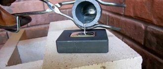
Melting alloy
Characteristics
It is worth noting that solder is undemanding to soldering equipment. This can be either a home option or industrial devices. Hence the prevalence of POS 40 both in everyday life and in enterprises.
Excellent for soldering on printed circuit boards with appropriate properties, as well as for creating a tight, reliable seam.
The density of this substance is 9300 kilograms per cubic meter. The diameter of the solder may vary. It varies from 0.5 millimeters to 3 millimeters. The mechanical tensile strength of this solder is 3.8 megapascals. Solder is produced in accordance with GOST.
Today on the market there are both tubes that already contain pine rosin, and wires that do not contain rosin. It is impossible to say which option is better - it all depends on the specific area in which solder is used. In some places the option with rosin will be preferable, and in others without.
Properties and markings
Finished alloys based on tin and lead have a number of properties that make the compound unique:
- Melting point - up to 500 degrees Celsius, depending on the percentage of alloying additives.
- High wear resistance.
- Oxidation resistance is higher than that of pure materials.
There are two types of lead compounds: babbitts and solders. The first ones are designated by the letter “B”. Next, the letters of the alloying additives, the percentage of the main substance, and the number of additional components are indicated.
Diameter of holes
Solder Solder T 2.0 POS 61 is POS solder in the form of a tube with flux with a diameter of 2 mm. Supplied in a coil or reel
Other markings are possible. For example, Solder POS-61-T1 And this is also solder POS-61, but in the form of a tube with a diameter of 1 mm
If you come across the marking Solder POS-61 (wire d-3 mm), then this is POS-61 solder produced in the form of wire with a diameter of 3 mm, without rosin, supplied in the form of a coil.
Marking Solder POS-30 or Solder POS-30 ⌀8 means the same thing. This is POS-30 solder, supplied in the form of a rod with a diameter of 8 mm.
Solder “A”, what is it for?
Solder “A” is a tin-zinc alloy, with the obligatory alloying additives of copper and aluminum. Used for tinning the aluminum cable sheath before applying PIC solder. Pre-treatment of the cable surface with solder “A” dramatically increases the electrical and mechanical strength of the soldered contact. However, applying solder "A" requires a lot of attention and skill. Solder “A” is a fairly refractory solder and there is a risk of overheating the cable sheath if unsuccessful attempts are made to rub it with solder “A”. It is very important to use a high-quality gas burner with adjustable flame sharpness for this.
Classification
Particularly common are alloys of tin and lead, called babbitts. They can be divided into several groups:
- Tin - designated as B83, B89. Contains antimony and lead. Tin acts as a base. Used in the manufacture of bearings for industrial equipment. However, the base metal is considered expensive, so cheaper analogues are often used.
- Lead - designated as B16. Lead-based alloys are considered more advantageous analogues of tin compounds. Their high wear resistance allows them to be used to make parts for machine tools and moving mechanisms.
- Calcium - solid particles that make up this alloy are a compound of calcium and lead. Tin acts as an additional component.
How to independently determine or decipher the brand of solder?
This solder is used to join copper-containing alloys using high-temperature soldering. It is highly plastic and durable, resistant to corrosion, and has high thermal and electrical conductivity. The melting point is directly proportional to the zinc content in it. The most common types of such solder: PMC-36, PMC-42, PMC-48, PMC-54. Their comparative characteristics are given in the table:
Tin-lead solders (the most common) are branded POS, if the composition also contains antimony (it increases strength) - POSSu. There are also tin-lead-cadmium (POSK), tin-zinc (TS) and lead-free solders. The most common brands:
Solders with a small silver content (PSr-1–25) are used for tinning and soldering of various metal parts. PSr30–45 allows you to obtain a more durable connection of elements made of copper and its alloys, nickel, kovar, bronze. Highly concentrated PSr-70 and PSr-72 have increased conductivity, tensile strength and bending strength. They are suitable for soldering band saw blades.
In most cases, deciphering the brand of solder is easy. The letter P stands for the word “solder”, the others stand for the components included in it (Sr – silver, K – cadmium, M – copper, A – aluminum, Kr – silicon, etc.). If the material contains precious and rare metals, marking begins with them, even if their share is only 1%. Next comes a figure corresponding to the percentage of the component. For example, PMC-36 contains 36% copper, POS-61 – 61% tin.
There are solders produced according to international standards, for example, Sn60Pb40 solder containing 60% tin and 40% lead. The melting point of 60/40 solder is 191 °C.
Solder performance can be improved by doping with the following substances:
POS-90 consists of 90% tin and 10% lead. It also contains about 0.1% antimony and 0.05% copper. Most often used for soldering and tinning internal seams of medical equipment and food utensils . The melting point of POS 90 is 220 degrees.
More homemade products: How to make a feed granulator with your own hands - steps with photos
Areas of application
Tin alloys were previously used to make dishes and cutlery. Nowadays they are much more often used to create cans. From this material, in combination with other components, solders are made, which come in several types:
- Low-melting - melting point does not exceed 150 degrees Celsius.
- Medium melting - become liquid when heated from 200 to 500 degrees.
- Refractory - melts at temperatures above 1100 degrees.
Another area of application for alloys is the production of friction-resistant parts.
Tin-lead solder
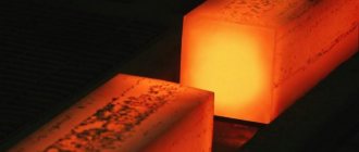
Features of production and processing
Consumable raw materials are obtained from ore. For example, to obtain 1 kilogram of pure material, it is necessary to process 100 kg of ore. Both materials melt at low temperatures. To manufacture the alloy, the following features must be taken into account:
- When making a casting mold, you must use a material that is not susceptible to wetting by molten consumable metals.
- The mold must withstand heating at temperatures above 250 degrees.
- Molten metals quickly oxidize when exposed to the environment. Solid metal is protected from oxidation.
When it comes to making solder, antimony is added to the compound. Some craftsmen add silver. It has the following features:
- Silver protects the material from rust formation.
- Due to the addition of noble metal, the price tag for finished solder increases, but its functionality expands.
There are solders with added zinc. However, they are rarely used. Zinc actively reacts to environmental factors. It begins to collapse, which leads to a violation of the integrity of the product. It is better to use a mixture of antimony, tin and lead. This solder is used to solder radio components, contacts, and wires. By changing components, craftsmen achieve the desired characteristics from a consumable. We must not forget about the use of flux.
The alloy of tin and lead has special characteristics. They change after adding alloying components. Ready-made compounds are used for the manufacture of solders, wear-resistant parts, dishes, cutlery, and cans.
Tin-lead coating structure.
4.1 Structure of the coating obtained from hydrofluoride electrolyte.
Let us consider the structural features of a tin-lead coating of eutectic composition (60% tin) from a fluoroborate electrolyte.
Figure 9 shows that lead is deposited on the tin, forming small islands. The deposition of lead clearly inhibits the deposition of tin on the tin, preventing the formation of dendrites.
Figure 9 - SEM images of a tin-lead alloy (60% tin) deposited from: a,c - 1mM Pb2+ + 10mM Sn2+, b,d - 2.6mM Pb2+ + 10mM Sn2+.
The strong influence of lead on the microstructure of tin can be correlated with insufficient deposition of lead on tin. This is also consistent with the fact that lead inhibits tin deposition, i.e. the tin has fewer areas available to grow and is difficult to deposit on the lead.
Figure 10 shows a backscattered electron image of a Sn-Pb(60) alloy.
Figure 10 - Backscattered electron image of a tin-lead alloy (60% tin) deposited from a solution of 2.6 mM Pb2+ and 10 mM Sn2+, at 550 mV for 300 s.
The gray areas of the crystals are tin, and the white part is tin. The crystallites have a fairly uniform distribution, and the curtains between the crystallites clearly show that material is being transferred to form larger units on the surface. In addition, lead and tin can be seen to be deposited side by side even in these small crystallites, showing alloy formation also on the microscale. The number of crystallites is approximately ten times greater than in the precipitate shown in Figure 9b.
However, the number of nucleation centers is still an order of magnitude lower than that obtained in potential stepwise experiments.
4.2 Structure of the coating obtained from a modern electrolyte without fluorine.
Figure 11 shows the surface morphology of a matte tin-lead coating deposited from a modern fluorine-free electrolyte, and Figure 12 shows a fluorine-free electrolyte.
Figure 11 — Surface morphology of a matte tin-lead coating deposited from a modern fluorine-free electrolyte.
Figure 12 — Surface morphology of a shiny tin-lead coating deposited from a modern fluorine-free electrolyte.
Figure 13 shows microimages of a 16-μm-thick Sn–Pb(98) coating 85 days after deposition from a state-of-the-art fluorine-free electrolyte.
Figure 13 - Low, medium and high magnification SEM images of the surface of a 16 µm Sn–Pb(98) coating on a cantilever beam after 85 days.
It can be seen that there are no tubercles or whiskers on the surface. Only grain boundary grooves are observed.
The SEM image in Figure 13c clearly shows four isolated Pb grains. This means that the Pb particles exist as individual grains mixed with the Sn grains, as in the fluoroborate solution.
A cross-sectional image obtained using a focused ion beam is shown in Figure 14. It shows that the structure of the Sn–Pb coating is not columnar. Compared to Sn and Sn-Cu coatings, Sn-Pb deposits have many more grain boundaries parallel to the top surface. Co-precipitation of Pb with Sn is known to significantly reduce any crystallographic texture of Sn, preventing columnar growth.
Figure 14 — Image of a thin section of a Sn–Pb(98) coating 16 μm thick, obtained using a focused ion beam.
SEM images of cross sections of 16 µm bronze with different coatings are shown in Figure 15.
Figure 15 - Sections of phosphor bronze 16 microns thick with coating: a - Sn; b - Sn-Cu; c — Sn-Pb(98) one year after coating.
Figure 15 confirms the columnar grain structure of Sn and Sn-Cu coatings. In all three microimages, a jagged intermetallic layer of Cu6Sn5 with a thickness of 1.5–2.5 μm is visible at the interface between the deposit and the substrate. A much thinner layer of Cu3Sn is also present, but it is almost invisible. In Sn-Cu coatings, the intermetallic Cu6Sn5 is also visible, distributed throughout the deposit, mainly along the boundaries of Sn grains.
No intermetallic compound is observed at the grain boundaries of the samples of pure Sn or Sn-Pb. Once again, we note the presence of a large number of transverse grain boundaries in the Sn-Pb deposit compared to the deposits of pure Sn and Sn-Cu. The location of the Pb phase was not detected in these micrographs.
Examination of the Sn-Pb(98) coating using a transmission electron microscope one day after deposition on glassy carbon showed extremely small, up to 10 nm spherical Pb precipitates. A month after coating, the Pb particles grow and appear as cuboids with tetragonal distortions of approximately 50 nm inside the grains and larger sizes at the boundaries of the Sn grains (Figure 16).
Figure 16 — TEM of the Sn–Pb(98) coating a month after deposition: a — Pb particles are tetragonally distorted cuboids approximately 50 nm inside Sn grains, b — larger Pb particles at the boundaries of Sn grains.
Figure 17 shows the effect of the grain refinement additive on the surface morphology of Sn–Pb(80).
Figure 17 - SEM showing the surface morphology of Sn-Pb(80) formed at: a - 10 A/dm2 from a bath with additives, b - 8 A/dm2 from a modern electrolyte without fluorine.
While the grains of a coating applied without a surfactant are very large and angular, the grains of a coating applied with an additive are very small and round.
The critical radius of the electrodeposited nucleus for stable growth is inversely proportional to the cathodic overvoltage. The nucleation rate also increases with cathodic overvoltage. Therefore, the higher the cathodic overvoltage, the smaller the grain size.
The cathodic overvoltage during Sn-Pb deposition in a bath with the addition of functional additives at 10 A/dm2 is 560 mV higher than without them at an equivalent current density. This leads to a smoother surface morphology of coatings from a bath with additives compared to a bath without them (Figure 18).
Crushing of embryonic grains is achieved using a pulsed current. The influence of the duty cycle and frequency of current pulses on the surface morphology of layers deposited at an average current density of 10 A/dm2 is shown in Figures 18 and 19, respectively.
Figure 18 - Influence of the operating cycle on the morphology of the surface deposited from a bath with Sn-Pb(80) additives at an average current density of 10 A/dm2 with a pulse repetition rate of 25 Hz.
Figure 19 - Effect of current pulse frequency on the surface morphology of Sn-Pb(80) deposited from a bath with additives at an average current density of 10 A/dm2 with a pulse repetition frequency of 25 Hz.
The surface morphology of the coatings appears to become rougher as the duty cycle or pulse frequency increases.