The need for this is faced mainly by those who use getinax samples with double-sided foil in their design. In order to subsequently assemble a working circuit on the board, you need to achieve high-quality electrical contact between its conductive layers. Judging by the reviews on the relevant forums, there are several proven and relatively easy to perform at home methods for metalizing holes in printed circuit boards.
This can be done in different ways, using certain reagents and techniques. Each experienced amateur craftsman has his own favorite technology. Let's look at the most common methods of silver plating and graphitizing holes at home. They are attractive not only because of their ease of execution, but also because of the availability of chemicals/preparations.
Metallization technology
Using this method of direct hole plating, you can achieve quality results when making double-sided printed circuit boards at home.
The main condition for 100% direct metallization of holes in this technology is the correct preparation of the dielectric surface activator based on the ammonia complex of copper hypophosphite and compliance with certain rules when activating the surface with this solution. How to prepare this activator based on copper hypophosphite for direct metallization of holes is described in detail in this article.
Direct metallization process
Next, the metallization technology will be described in the form of a photo gallery with some explanations. All photos are clickable. You can also hover your mouse over the photo and read its description in a pop-up window.
I want to say right away that this scarf is a test one and was made only to describe this process.
Drilling holes
So we take the textolite and prepare the surface for applying photoresist (on one side). We glue the photoresist to one side, take a photomask with the centers of the future board holes, expose it, and develop the photoresist (unfortunately, I couldn’t photograph this stage, but I think everything is clear here). As soon as the photoresist has been developed, we glue tape on the other side of the board to protect the copper and etch the board in ammonium persulfate or ferric chloride:
The scarf has become etched, the photoresist needs to be washed off. To do this, we throw the board into caustic soda (NaOH) or the “Mole” solution for 10 minutes, then the photoresist is easily washed off from the surface of the board. You don't have to wash off the photoresist at this stage, but wash it off after drilling the holes. As soon as the photoresist is washed off, the centers of future holes are visible on the copper foil, so we drill holes along them using a machine or manually. After drilling the holes, there will be burrs on the other side of the PCB that will need to be removed:
To do this, sand the board on both sides with fine sandpaper, then use a needle in a circular motion to straighten the holes and thereby remove the remaining burrs. After this, sand the printed circuit board again with fine sandpaper:
Dielectric activation
At the next stage, we take ammonium persulfate and the prepared activator solution based on copper hypophosphite. First, we etch the board in ammonium persulfate for 20 seconds (to give the copper a smooth roughness), then, without touching the copper with your fingers, rinse the board in water and immerse it in the activator solution for 1 minute. The scarf in the solution must be constantly shaken so that the holes are guaranteed to be filled with the activator.
We remove the board from the activator, let the excess solution drain from the surface and, without shaking the board off (the most important thing is that the holes are filled with the activator), we perform a thermal shock (heating) in any available way at a temperature of 150 degrees for 10 minutes. The most important thing in this process is to ensure that the solution does not boil away from the holes, but evaporates evenly.
At the end of the thermal shock process, the board will darken, which is a sign of successful decomposition of copper hypophosphite into metallic copper, onto which direct metallization will be performed:
Preparing the board before electroplating
After the thermal shock, let the board cool, then, if necessary, clean the holes with a needle and be sure to wash it with detergent. We don’t touch the printed circuit board with our hands:
PCB electroplating
We lower the board into the galvanic bath and begin the process of direct metallization. We keep the board in the galvanizer for about 2 hours, constantly shaking the board, the current is 2 amperes per square meter. We finish the copper coating process, take out the board and look at the quality of the metallization, it is 100%. Sand the surface with fine sandpaper:
We form the tracks of the printed circuit board
Now let's move on to the actual manufacture of the printed circuit board itself. To do this, we glue photoresist to one side of the printed circuit board, prepare a photomask without the centers of the holes, align it on the board along the holes, expose it and develop it. We make sure that the holes are properly covered with photoresist awnings (if the awnings are torn, then fill the holes with varnish), otherwise after etching in ferric chloride, the metallization in these places will be etched and all the work will go down the drain:
After developing the photoresist, we illuminate the scarf again to better fix the photoresist. We cover the back side of the board with tape and etch it in ammonium persulfate or ferric chloride.
In general, you can skip this step, that is, initially glue the photoresist on both sides, expose and develop it, then etch both sides of the board in ferric chloride at the same time:
This article was published on the website whoby.ru. The permanent link to this article is at this address https://whoby.ru/page/metgfmed
Read articles on the original site, do not support thieves.
As we did one side, we do the same on the other side of the printed circuit board. We glue the photoresist, align the template with the holes, expose it, and develop it. After development, we look at the quality of the awnings over the holes; if some are torn, then we correct them (with varnish), then we expose them again:
We seal it with tape and etch it in persulfate or ferric chloride. Then we take caustic soda (NaOH):
And we wash off the photoresist on both sides of the board. We look at the quality of metallization, mordant under the awnings (if any). Everything is in order, now the board needs to be coated with tin.
Tinning boards with rose alloy
In order for the tin to properly cover the conductors, you need to prepare the surface of the copper. To do this, we throw the board into a solution of citric acid, 20 ml of water, a teaspoon of lemon, to clean it from oxides.
Then we prepare a solution in which we will tin the board. Why take one bottle of glycerin 20 ml. 100 ml of water and a teaspoon of citric acid. Then this solution is heated to a boil and the Rose alloy is added to it:
We lower the board into the solution and cover the conductors with tin using sponge movements. The main thing at this stage is to fill all the holes with tin. Then we take the board out of the solution and heat it over gas until the Rose alloy melts. As soon as the alloy is melted, quickly shake off the excess solder from the holes. It is important that there is no solder left in the holes, to do this we look at the clearance:
Once again, dip the scarf into the glycerin solution, but without the Rose alloy in it, and heat it to a boil. Use a sponge to remove excess solder from the conductors. If one or more holes are filled with tin again, then repeat the shaking operation. The result is this nice scarf with metallized holes:
Conclusion
As you can see, there is nothing complicated about direct metallization of holes using copper hypophosphite. The boards are of decent quality.
I advise you to first try this direct metallization technology on small boards first, so that you gain experience, and only then make more complex boards.
The founder of this activation method is a group of chemists from the Novosibirsk Institute of Solid State Chemistry and Mechanochemistry, headed by Oleg Ivanovich Lomovsky . She received the latest patent for this technology.
A lot of work was done in the development of this technology by user JIN from the vrtp.ru (link to the forum topic). Thanks to which this method reached the masses of radio amateurs.
NTD on metallization
According to IPC, H:d (aspect ratio) is defined as the ratio of the thickness (of printed circuit boards) to the minimum diameter of the drilled hole (drill diameter).
According to the domestic GOST 23 751 -86 - H:d (or the reciprocal value - γ) was defined as the ratio of the thickness (of printed circuit boards) to the minimum diameter of the metallized hole, i.e. at least 0.05 mm smaller (in GOST R 53429-2009, which replaced it), there is no mention of “aspect ratio” at all.
Note. Nevertheless, for a sufficiently deep understanding of the content of articles and documents, it is necessary to understand that the domestic standard corresponded to the smaller IPC standard, especially for small diameters (for example, H: d = 20: 1 or γ = 0.05 according to domestic technical specifications for a drill diameter of 0, 15 mm corresponds to H:d=13.5:1 according to IPC).
Another parameter characterizing the metallization of holes is the distribution of applied copper along the length of the hole (TP - English abbreviation). This parameter allows us to evaluate the ability of the plating process (especially for small hole diameters using direct plating) to deposit a sufficient thickness of the plating column without inadequately narrowing the lumen of the hole. Unfortunately, domestic normative and technical documentation does not specify this value in any way. In Fig. 94 shows two options for estimating the distribution:
— according to IPC – the most accurate;
— operational (TPMIN), often used by practicing technologists for quick assessment.
Figure 94. Options for calculating the distribution of metallization thickness
GOST 23752 specifies the minimum permissible average metallization thickness for double-sided printed circuit boards - 20 microns, for multilayer printed circuit boards - 25 microns.
Copper hypophosphite (activator solution)
Diamincopper hypophosphite dihydrate two
Solution: Calcium hypophosphite (calcium hypophosphate) - 20 g. [Ca(PH2O2)2] Copper sulfate (Copper 2 sulfate 5 water) - 25 g. [CuSO4 5H2O] (by the way, sold in gardening stores) Ammonia (pharmacy 10%), = 10% aqueous solution of ammonium hydroxide - 50 ml. (NH3+H20) Distilled water 100 ml. Detergent “Drop” - 3 g. (water, surfactant, sodium chloride, preservative, perfume composition, citric acid, SI 19140, 42090)
1. Copper sulfate 25g + water 50ml = long (+ sediment) 2. Calcium hypophosphite 15g + water 50ml = long 3. 1 pour into 2. (mix) = + sediment 4. filter (discard sediment) 5. + 50 ml. pharmaceutical 10% ammonia 6. + 5 grams of calcium hypophosphite 7. + detergent (liquid soap) - 3 grams
We clean the board with an abrasive detergent without fanaticism, and wash it thoroughly.
At the end of the washing, the water should “stick” to the workpiece, flowing off it extremely reluctantly.
Shake it thoroughly, lower it horizontally into the activator, without touching the bottom.
Remove it horizontally to the surface several times for 2-3 seconds.
The liquid should flow evenly into all holes
We tilt it and touch the edge of the container so that the excess activator flows back (without fanaticism).
Close the container with the activator and tilt it at different angles, trying to allow the activator to spread as evenly as possible.
Then we put it in the oven, set it to 125C and keep it for 12-15 minutes.
Then 175C and hold for 7-8 minutes, open the door and let it cool down to 100C.
We can easily wash it with a non-abrasive detergent and a soft sponge (without water yet).
Use a washcloth to push the detergent through all the holes, calmly and slowly, trying not to miss anything.
Next, use a stream of water to rinse all the holes. no need to wash every single stain.
The activator can be stored for a long time, the main thing is that the ammonia does not evaporate from it, that is, we store it hermetically (in the dark). This means the container is better - a bottle with a minimum of space not occupied by liquid. I kept it on the balcony for a month and it reached -10C. I used it 10 times without problems (the properties of the activator were preserved).
The activator is stable and can be stored for a long time. During use, you need to ensure that there is always a sediment of calcium hypophosphite at the bottom and, if necessary, add a couple of grams. If this is not done, unplated holes may appear.
Calculating the impedance of differential vias
The calculation of differential p/o is similar to single ones, except that now we do not have a calculator: the above tools do not calculate differential p/o.
Also, now we can additionally change the step p/o in differential. couple Let's take the same structure: an 8-layer board with a thickness of 1.6 mm. Let's consider 9 p/o configurations (Figure 15).
The first 3 p/o have gaps of 0.125 mm and differ only in the location of the holes for the return current. All p/o from 4 onwards have a pitch of 1 mm. P/o from 6 onwards have an increased anti-fall (0.250 mm) and differ in the indentation of the holes for the return current.
Figure 15. Vias.
Consider the impedance graph (Figure 16).
Figure 16. S/O impedance in the time domain.
The “hump” is clearly visible on the graph, which corresponds to the vertical segment of the p/o - “glass” (English: Via barrel).
Having examined the frequency dependence of the reflection coefficient of VIA1-3 (Figure 17), we see that despite good performance at the target frequency of 6 GHz, there is resonance at lower frequencies. It is preferable to improve via7-9, and if that doesn’t work, then via4-5 in order to reduce the “hump” by shifting the graphs to the right.
Figure 17. Reflection coefficient from the p/o input.
Let's reduce the anti-fall on VIA9 to get gaps of 0.125 mm. For VIA4, let’s reduce the p/o step to 0.75 mm and consider the result obtained (Figure 18).
Figure 18. Impedance comparison of modified p/o.
In the frequency domain, a shift of the reflection coefficient graph from the input to the right is visible (Figure 19).
Figure 19. Comparison of reflectance of modified p/o.
electrolysis
Solution: 10 g. copper sulfate dissolves in 100 ml. add 1cm3 (=1ml) of water (electrolyte for lead car batteries) = sulfuric acid solution
RV-T shine additive if possible.
The electrodes must be completely covered
Capacity: in the middle the cathode is MINUS (our board), moves left / right (Arduino + servo motor on the plastic insides of a CD ROM) on the sides the anode is PLUS.
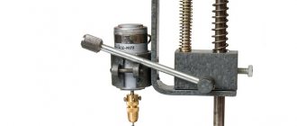
We give a current of 2A per 1 dm2 of board. My first electrolysis setup looked like this:
The electrolyte lives for a long time, the main thing is to keep it clean (filter through cotton pads or gauze). I store the electrolyte in a regular plastic food container (you can store it anywhere).
It is clear that you cannot use the stove for cooking. I tried to heat the board on the stove and, due to inexperience, overcooked the board until the PCB softened - the stench was terrible. I had to buy a regular stove for $25 (up to 250C) and immediately the process went in the right direction. Result after 10 minutes of electrolysis. Unfortunately, MINUS was applied only to one side of the board (the second was without potential), but I must admit everything is very encouraging:
holes 0.4mm
I took photos using a flashlight from below.
As a result, we must conclude that copper is deposited in the holes, although not evenly enough (there are noticeable bald spots).
An unnecessary effect is also the deposition of copper on the entire flat surface of the board, increasing the already sufficient copper thickness of 0.35mm. The fact is that copper is consumed quite intensively and the Anode disappears before our eyes.
Maybe it makes sense to cover everything with a mask of something and leave only holes?
manual metallization without chemicals
LPKF advertises a miracle paste for metalizing holes without chemicals, i.e. without electrolysis. Just rub the paste into the holes and heat the board. But you can’t find it in the public domain on the Internet, and of course not on Ali either.
Upon request, prices for Russia were sent as follows:
Complete set: 115790 ProConduct metallization basic set € 970.00.
Or its components:
116110 Polymer paste for ProConduct 20x2.9g. € 222.00
116159 ProConduct foil consumable set (Films) € 109.36
115891 LPKF – Cleaner for ProConduct € 37.38
Factor 2. Parasitic inductance and capacitance
Conductors on a printed circuit board can be made with a characteristic impedance that lies in a wide range, but most often it is 50 Ohms.
On the one hand, this is due to historical continuity: 50 ohm impedance was standardized for coaxial cables as a compromise between driver load level and signal energy loss. On the other hand, a 50 ohm conductor is easy to fabricate on a standard board. What is important for the developer is not so much the specific value of the wave impedance, but rather its constancy throughout the entire transmission line.
In order to make a transmission line with a fixed characteristic impedance value, the designer selects the width of the track and the distance to the supporting layer, i.e. changes the linear capacitance and inductance of the transmission line to a certain
quantities.
In p/o the inductive component is quite significant. As a first approximation, we must, within reason, reduce the parasitic inductance as much as possible, and then change the p/o parameters to achieve the given
capacitance, and accordingly impedance.
An excessive decrease in the capacitance of the p/o will cause a local increase in impedance and, as a result, signal reflections.
What keywords are we looking for on the Internet?
Pcb plating foil protection film hot air convection oven pcb plating pasteber conductive copper paste plum electrically conductive paste Carbon Conductive Assembly Paste Through-Hole Plating With Rivets Chemical-Free Through-Hole Plating Through-Hole Electroplating Galvanization liquid tin Immerse tin plating
No-clean, lead-free solder paste is a modified rosin based paste, which allows repeatability and consistency. The Patented Nihon Superior nickel stabilized tin/copper eutectic alloy has a melting point of 227°C. Size: 250 gram jar
Metallization of holes in pictures (part II, preparation for electroplating)
Continuation of the description of the process of metallization of holes at home, begun in the first part.
Reminder: WE WORK WITH GLOVES! In relation to this stage, IT IS IMPORTANT TO REMEMBER THE FOLLOWING: 1. DO NOT TOUCH THE BLANKET WITH YOUR HANDS, EVEN WITH GLOVES! 2. AN OPEN CONTAINER WITH AN ACTIVATOR IS A SOURCE OF AMMONIA! KEEP YOUR HEAD AWAY FROM HER!
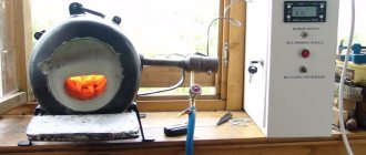
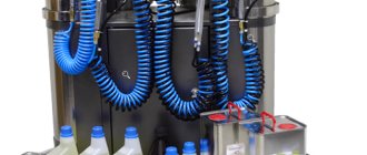
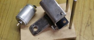
Appliances and tools: 1. Electric oven or convection oven. They are required to be able to quickly regulate the temperature. If you have a thermostated (at least up to +-5 degrees) furnace or a furnace capable of withstanding temperatures according to a given profile (for example, a purchased/homemade furnace for SMD soldering), this is even better. If there is no such oven and, at best, there is only a “display meter” in the form of a regulator or thermometer with an accuracy of +- half an elephant, then you will also need a thermometer capable of measuring temperatures in the range of up to 200 degrees. A thermocouple and tester are fine.
2. Medical clamp (preferably long). For those who don't know, this thing looks like this:
Materials: 1. Mild abrasive detergent.
2. Detergent without abrasive.
Here is the set of detergents that I currently use:
Factor 5. Interference in the power buses
In addition to adjacent signal circuits, signal quality can be affected by interference from internal layers.
Large currents can flow through power supply areas. Due to the increase in inductance at the edges of the polygons, flowing currents form fringing fields along all boundaries of the polygon, including in cutouts. Edge fields are a source of electromagnetic radiation (edge-fired emission) into space. To reduce the emission of electromagnetic radiation, the 20H rule is applied (Figure 8), which consists of narrowing the power polygon in relation to the ground polygon.
Figure 8. Edge fields and the 20H rule.
To protect the power supply from interference, if possible, it is necessary to increase the anti-fall at power supply areas. The 20H rule for p/o is difficult to provide, and also unnecessary; an anti-pad with a diameter of about 2 mm is usually recommended (Figure 9).
Figure 9. Increased anti-fall on power layers
Metallization of PCB vias with cable lugs
I remember in childhood, when we made foil getinax ourselves, using BF glue and an iron, we had a dream - hollow rivets.
Some magazine published the technology for their production. It was proposed to stretch a strip of foil through a conical hole (similar to a spinneret board) to form a tube. Then you need to cut a tube and rivet it on both sides in the board.
It seems that the article was incomplete, because I still have difficulty imagining how it can be put into practice at home, starting with making a die.
A lot of work was spent, but nothing worthwhile came of it. The configuration of the die must be complex, the working surface must be polished, the workpiece for it must be hardened, and most importantly, the width of the strip must be maintained with fairly high accuracy. Cutting the resulting tube is another task, and riveting it is also quite difficult.
Recently I needed to make a double-sided printed circuit board. And not just double-sided, but always with transitions between layers, since when soldering there will be no access to the opposite side. And not just with transitions, but with fairly powerful transitions, because relatively large currents are supposed to flow through these transitions.
The first thought was to make additional platforms and connect the layers with copper rivets from a suitable wire, but the subconscious protested - the solution was clumsy...
but somehow I didn’t associate them with rivets, until the insulator fell off at one tip...
This is where everything fell into place. At the first moment, all kinds of flaring with a shaped working part began to come to mind, highly desirable, made of hardened steel, with a polished surface. But, in the end, I decided not to bother and work with the tools at hand.
Factor 4: Crosstalk
Crosstalk is the unwanted transmission of a signal from one line to another.
This transfer occurs because two closely spaced conductors have capacitive and inductive coupling. The nature of crosstalk between signal conductors and p/o is slightly different. In the s/o, the signal does not have a supporting layer; return currents flow through adjacent s/o, forming a large loop. Crosstalk of signals in the p/o is caused by the inductive component.
The greatest effect in minimizing crosstalk can be achieved by increasing the distance between the p/o. However, often the topologist does not have much space.
The proximity of the p/o in a differential pair not only reduces the occupied area, but also has a positive effect on noise immunity [3].
A common way to minimize crosstalk between adjacent signal terminals is to place a shielding terminal between them. With this method, you will need to conduct signals in increments of about 2 mm (Figure 6). If there is not enough space, you can use a smaller step with a shift (English Staggered pattern), as in Figure 7. Using simulation, you can select the ideal shear angle [4].
Figure 6. Minimizing crosstalk using shielding P/O.
Figure 7. Minimizing crosstalk using diagonal checkerboard shift.
Crosstalk can also be reduced by exotic methods, for example, a long stub (by shifting the inductive-capacitive balance of the p/o) [5]. Interference can also be reduced at the design stage of the chip package [6].
↑ Tool
Wire cutters, pliers, hole punch and hammer. A cone awl is an important tool in this matter. I had a drill sharpened in time immemorial (now I can’t even imagine why) - it just fit. Well, and most importantly, a multifunctional tool, commonly called a “tin can,” which plays the role of an anvil.
Experiments have shown that the result is quite functional, not factory-made, of course, but this does not matter - the uneven edges of the rivets are hidden under the solder.
↑ Implementation
We insert the flared tube into the board. It is better if the hole in the PP corresponds as much as possible to the outer diameter of the tip tube; the tube should fit tightly, with difficulty. Press down as much as possible with your fingers. I did not use a special tubular upsetting with a hammer. The resulting margin resulting from incomplete contact of the flaring with the board is precisely used for flaring the rivet on the other side of the board.
We bite the rivet flush with the foil. As practice has shown, it is best to bite with side cutters with flat (without chamfer) cutting surfaces.
The tube naturally shrinks when cut, I tried, before biting, to insert a piece of winding wire inside the tube, but the result was not very foldable. It turned out that it was much easier to insert a suitable conical awl from the flaring side and straighten out this compression.
The rest is quite simple. All that remains is to take the core and flare the resulting rivet.
A couple of light blows on the protruding edges and a brand new rivet is in place. Sometimes, depending on the situation, it is necessary to slightly widen the hole with a conical awl.
Cutting the tip - lightly compress the flattened tube with pliers,
Straighten with an awl, insert into the board and flare the straightened end
Getting a new blank for a hollow rivet
And then - everything in a circle... Here is the result - the board is one-sided
On the other side
On the other side.
The board contains exactly the parts that started the whole thing.
I hope my idea of using cable lugs will be useful to fellow citizens. Thank you for your attention!
Signal integrity
Via holes (hereinafter referred to as via) represent inhomogeneities in the transmission line.
Like other inhomogeneities, they spoil the signal. This effect is weakly expressed at low frequencies, but increases significantly with increasing frequency. Often, developers pay undeservedly little attention to the structure of vias: they can be copied from a “neighboring” project, taken from a datasheet, or not specified at all in CAD (the default setting). Before using the calculated structure, you need to understand why it was made that way? Blind repetition can only do harm.
The signal integrity of a channel as it passes through vias is primarily affected by the following factors:
- signal reflections due to changes in wave impedance;
- signal degradation due to parasitic capacitance and inductance;
- reflections from an unused segment of the p/o when moving to the inner layer (hereinafter stub from the English via stub);
- crosstalk (eng. Cross talks);
- interference in the power buses.
Let's take a closer look at the causes of these effects and methods for eliminating them.
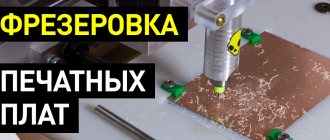
Metallization of printed circuit board holes at home - step-by-step instructions
The need for this is faced mainly by those who use getinax samples with double-sided foil in their design. In order to subsequently assemble a working circuit on the board, you need to achieve high-quality electrical contact between its conductive layers. Judging by the reviews on the relevant forums, there are several proven and relatively easy to perform at home methods for metalizing holes in printed circuit boards.
This can be done in different ways, using certain reagents and techniques. Each experienced amateur craftsman has his own favorite technology. Let's look at the most common methods of silver plating and graphitizing holes at home. They are attractive not only because of their ease of execution, but also because of the availability of chemicals/preparations.
Hole preparation
Fig.95. Hole after excess plasma treatment.
There are 3 known methods for preparing holes:
— Permanganate treatment (cheap and relatively effective, but has restrictions on DE brands - it does not etch fluoroplastic at all and does not work well with polyimide).
— Plasma-chemical preparation (requires complex engineering support and highly qualified personnel). For fiberglass laminate, with prolonged exposure or the selection of aggressive frequency modes, the DE is greatly reduced, forming a “brush” of glass fibers inside the hole (Fig. 95). In this case, the metallization column partially filled with the tips of glass fibers acquires increased resistance compared to solid copper.
— Pickling in compositions with hydrofluoric (or other concentrated) acid (an outdated and very harmful method for personnel; today it is practically not used in real production).
Silvering
Preparatory activities
The technology is based on the fact that under the influence of ultraviolet light, silver nitrate (better known as lapis AgNO3) decomposes into components, one of which is pure metal.
- The holes in the board are cleaned.
- Each of them is treated with a solution (25±5%) of silver nitrate.
- Next is drying the printed circuit board. To speed up the chemical reaction, it is advisable to use a UV lamp for these purposes. As a result, only isolated inclusions of silver will remain on the getinax (in the area of the holes).
Obtaining a conductive layer
For this you will need copper. It is obtained from solution. The metal is deposited on a prepared “base” of silver, thereby subsequently ensuring reliable electrical contact between all elements of the circuit.
This solution is extremely unstable and its shelf life is limited. Therefore, it makes no sense to prepare the drug in reserve. Only in the required quantity and before direct use, when the initial processing of the holes (silvering) has already been completed. The percentage of components depending on the required volume of solution can be easily calculated using the given recipe.
Reinforcing holes
Complete metallization is sufficient only if, when installing an electronic circuit, you intend to work with miniature radio components. But, as practice shows, one layer is enough. Consequently, there is no longer any need to talk about the maintainability of the printed circuit board. That is why the thickness of the metallized layer is increased by galvanic methods, such as nickel plating, for example.
- “Minus” is on the foil covering of the board, “plus” is on the copper plate. It is located parallel to the sample being processed.
- Current density (A/cm2) is selected in the range 0.02 – 0.3.
- Voltage (V): 3.5±0.5.
- Acceptable temperature (ºС) in a galvanic bath is from 20 to 28.
A higher quality, homogeneous layer is obtained with lower current. But this increases the time of the process of metallization of holes.
Graphitization
Another easy-to-use metallization method. The difference is that for the initial processing of holes, instead of silvering, graphitization is done. Most often, amateurs use store-bought aerosol CRAMOLIN “GRAPHITE” . It is enough to press the finely dispersed fractions of graphite deposited on the surface into the prepared holes. This is easy to do with a small spatula or scraper. There is no need to explain how to make them yourself.
To remove excess, while the paste is still wet, shake the board. Fractions adhering to its surface are washed off with a solvent or removed with fine (grinding) sandpaper. All that remains is to clean the hole with a thin needle.
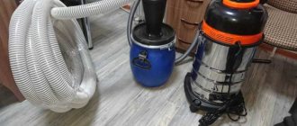
As a result, it produces the thinnest conductive layer. This method of removing paste has a disadvantage - not all fractions are removed from the hole, which reduces its diameter. A better result is achieved by the blowing method. At home, you can use a vacuum cleaner.
The described methods for metallizing holes are not the only ones. But it was the author who tested them at one time, and they proved their effectiveness and ease of implementation.
Factor 1. Characteristic impedance p/o
In an ideally designed board, the wave impedance does not change throughout the entire route, including when moving to another layer. In reality it usually looks something like this:
Figure 1. Change in wave resistance when moving to another layer.
The better the wave impedances are matched, the less signal reflection will be. How can we influence this?
Let's consider the structure of the p/o on the board [1].
Figure 2. P/O structure on the board.
| Layer | Element | Property |
| TOP | P/o site | Parasitic capacitance between the pad and the L2 power supply area |
| TOP-L2 | section p/o | Inductance |
| L2 (power area) | Antipad | The anti-pad forms an edge capacitance - a capacitance between the walls of the p/o and the power supply area |
| L2-L3 | Section p/o | Inductance |
| L3 (power area) | Antipad | The anti-pad forms an edge capacitance - a capacitance between the walls of the p/o and the power supply area |
| L3-L4 | Section p/o | Inductance |
| L4 (signal) | P/o site | Parasitic capacitance between the power supply area and the L3 power supply area |
| L4-L5 | Stub | Noise Source |
By changing the elements of the junction, we change the characteristic impedance of the junction. Our goal is to match the impedance of the transition structure to the impedance of the conductors to minimize reflections. Let's consider how the impedance changes when the elements of the p/o structure change.
| Element | Action | Electrical property | Impedance (result) |
| P/o site | ↓ | C↓ | ↑ |
| Diameter of p/o | ↓ | L↑ | ↑ |
| Antipad | ↑ | C↓ | ↑ |
| Length | ↑ | L↑ | ↑ |
| Number of power supply polygons along the route | ↓ | C↓ | ↑ |
| Step p/o | ↑ | C↓ | ↑ |
| Distance to return points | ↑ | L↑ | ↑ |
| Number of returnable items | ↑ | L↓ | ↓ |
| Filling holes | Fill with resin (Dk↑) | C↑ | ↓ |