Field effect transistor - what is it
It includes three main elements - source, gate and drain. To create them, n-type and p-type semiconductors are used. They can be combined in one of the following ways:
- The drain and source are n-type and the gate are p-type. They are called npn type transistors.
- Those that use pnp polarity. The type of conductivity of each part of the transistor has been changed to the opposite in comparison with the previous version.
Checking with a multimeter
If this part is connected to a power source, then there will be no current. But everything will be different if this is done between the source and the gate or the drain and the gate. It is necessary that a voltage be applied to the gate corresponding in sign to its conductivity type (positive for p-type, negative for n-type). Then current will flow through this part. The higher the voltage applied to the gate, the stronger it will be.
The difference between a field-effect transistor and a bipolar transistor
The transistor will become open provided that a potential difference of the required polarity is applied to the gate. In this case, with the help of an electric field, a channel is created between the source and drain, through which electric charges can move. Other types of transistors control based on current rather than voltage.
The electronic components in question are also called mosfets. This word comes from the abbreviation MOSFET - Metal Oxide Semiconductor Field Effect Transistor (translated this means: metal-oxide-semiconductor field-effect transistor).
Varieties of field beetles
Device details
Matching transformer: W-shaped core, with a cross-sectional area of at least 2 sq.cm. Both windings are wound with PEV-2 wire with a diameter of 0.1 mm. The primary winding consists of 2300 turns, the secondary winding of 644 turns with a tap from the middle of the winding.
When winding, it is advisable to first wind the secondary winding, then insulate it and wind the primary on top of it. You can also use a ready-made miniature transformer from a radio receiver. Usually they come in USH12.5X20 or Sh12X16. Capacitor C1 - K73-5.
The following types of headphones TK-47, TA-56M, TA-4 can be used as an audible alarm.
Source: Homemade electronic devices for the home, Sidorov I.N.
How does it work
The field-effect transistor differs from other varieties in the features of its device. It can be one of two types:
- with control transition;
- with insulated shutter.
The first of them are n channel and p channel. The first of them are more common. They use the following operating principle.
A semiconductor with n-conductivity is used as a basis. The source and drain contacts are connected to it on opposite sides. In the middle part, on opposite sides, there are inclusions of a conductor with p-conductivity - they are a gate. The part of the semiconductor that is between them is a channel.
You might be interested in everything about phase-zero loops
Transistor with control junction
If a potential difference is applied to the source and drain of an n channel transistor, then current will flow. However, when a negative voltage is applied to the gate relative to the source, the channel width for electron movement will decrease. As a result, the current strength will become less.
Thus, by decreasing or increasing the width of the channel, it is possible to regulate the current strength between the source and drain or isolate them from each other.
In p-channel transistors, the operating principle will be similar.
This type of FET is becoming less common, and is being replaced by those that use an insulated gate. They can be one of two types: npn or pnp. Their operating principle is similar. The first of them will be discussed here in more detail: npn.
In this case, a p-type semiconductor is used as the basis for the transistor. Two parallel strips of semiconductor with a different type of main charge carriers are built into it. An insulator is laid between them on the surface, and a layer of conductor is installed on top. This part is the gate, and the strips are the source and drain.
Transistor device
When a positive voltage is applied to the gate relative to the source, a positive charge is applied to the plate, creating an electric field. It attracts positive charges to the surface, creating a channel for current to flow between source and drain. The higher the voltage applied to the gate, the higher the current flows between the source and drain.
For all types of field-effect transistors, control occurs by applying voltage to the gate.
Transistor open
A little about the design
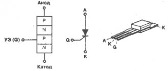
The field effect transistor consists of the following elements:
- n-channel, which has a silicon substrate with p-conductivity;
- n-regions, which are obtained by adding impurities to the substrate;
- insulating the gate from the dielectric channel.
Pins are connected to n-areas. Current flows from source to drain through the transistor thanks to the power supply. The amount of current is controlled by the insulated gate of the transistor.
When working with a transistor component, you must consider its sensitivity to the effects of an electric field . Such elements should be stored with the terminals short-circuited with foil, and before soldering they will need to be short-circuited with wire. Soldering of transistor elements is carried out using a soldering station that provides protection against static electricity.
Before deciding how to test a mosfet with a multimeter, you need to determine its pinout. The imported device has marks corresponding to the terminals of the transistor. In this case, the letter G denotes the gate of the device, S is the source, and the designation D refers to the drain.
What malfunctions occur
Field-effect transistors can be overloaded with current during testing and, as a result of overheating, become faulty.
Important! They are vulnerable to static voltage. During the work, you need to ensure that it does not fall on the part being tested.
When working as part of a circuit, a breakdown may occur, as a result of which the field-effect transistor becomes faulty and must be replaced. It can be detected by the low resistance of pn junctions in both directions.
You can determine how efficient a transistor is by testing it with a digital multimeter.
Pin assignment
This should be done as follows (for example, the widely used M-831 model is used, a field-effect transistor with an n-type channel is considered):
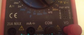
- The multimeter must be switched to diode test mode. It is marked on the panel with a schematic diagram of a diode.
- Two probes are attached to the device: black and red. There are three slots on the front panel. Black is set to the bottom, red to the middle. The first of them corresponds to the negative pole, the second to the positive pole.
- It is necessary to determine on the field-effect transistor being tested which outputs correspond to the source, gate and drain.
- Some models additionally have an internal diode that protects the part from overload. First you need to check how it works. To do this, the red wire is connected to the source, and the black wire to the drain.
You might be interested in How to measure voltage
Checking the diode in the forward direction
A value within the range of 0.5-0.7 should appear on the indicator. If the wires are swapped, the screen will indicate one, which means that no current flows in that direction.
Diode test in reverse direction
- Next, the functionality of the transistor is checked.
If you connect the probes to the source and drain, then the current will not pass through them. To open the shutter. A positive voltage must be applied to the gate. It must be taken into account that a positive potential is applied to the red probe from the multimeter. Now it is enough to connect it to the gate, and the black one to the drain or source, so that the transistor begins to pass current.
Channel opening
Now, if the red wire is connected to the source, and the black wire to the drain, then the multimeter will show a certain voltage drop value, for example, 60. If you connect it the other way around, the indicator will be approximately the same.
If a negative potential is applied to the gate, this will turn off the transistor in both directions, but the built-in diode will work. If the field switch does not close, this indicates its malfunction.
Checking the p-channel mofset is done in a similar way. The difference is that when testing where previously a red probe was used, a black one is now used and vice versa.
Operation of a field-effect MOS transistor
Determination of the functionality of an n-channel semiconductor.
Since such components often have a diode built in between the drain and source, to check functionality, the measuring device is set to diode test mode. H goes to the minus of the tester, and K goes to the plus.
- K is placed at the source of the element, and H at the drain. The voltage should be between 500 and 700 mV.
- K is for drain, and H is for source. The value in this case should be outside the measurement range of the multimeter. This is indicated by the number “1” on the device screen.
- H - at the source. Touching the gate K opens the transistor. H remains at the source, and K is connected to the drain. The measured voltage should be in the range from 0 to 800 mV and should not depend on the change in polarity of the tester wires.
- Closing K to the source, and CH to the gate leads to the closing of the device and transferring it to its original state.
To determine the performance of a p-channel semiconductor, H is connected to the plus of the multimeter, and K to the minus. The further sequence of actions is similar to the procedure for checking an n-channel element.
Instructions for dialing without soldering
To check whether the field-effect transistor is working, you need to unsolder it and test it with a multimeter. However, situations may arise when you need several such parts in the circuit and it is not known which of them are working and which are not. In this case, it is useful to know how to test a field-effect transistor with a multimeter without desoldering.
Digital multimeter
In this case, a test without desoldering is used. It gives an approximate result.
Important! After the presumably faulty element has been identified, it is disconnected and checked, obtaining accurate information about its performance. If it functions normally, it is installed in its original place.
Testing without desoldering is performed as follows:
- Before testing the field-effect transistor with a digital multimeter, disconnect the device from the electrical outlet or from the batteries. The latter are removed from the device.
- If the red probe is connected to the source, and the black probe to the drain, then you can expect that the multimeter will show 500 mV. If you can see this figure or one that exceeds it on the indicator, this indicates that the transistor is fully functional. If this value is much less - 50 or even 5 mV, then in this case a malfunction can be assumed with a high probability.
You might be interested in this Classification of electrical circuits
With control pn junction
- If the red multimeter probe is moved to the gate, and the black one is left in the same place, then the indicator will show 1000 mV or more, which indicates the serviceability of the field-effect transistor. When the difference is 50 mV, this raises concerns that the part is damaged.
- If the black probe of the tester is placed on the source, and the red probe is placed on the gate, then for a working transistor you can expect 100 mV or more on the display. In cases where the figure is less than 50 mV, there is a high probability that the part being tested is inoperative.
It must be taken into account that the conclusions obtained without soldering are probabilistic in nature. These data allow us to draw preliminary conclusions about the field-effect transistors used in the circuit.
To check, they need to be unsoldered, checked and installed if the functionality is confirmed.
Preparing for work
Is it possible to check the transistor on the board?
This means that the collector and emitter junctions are intact, which means that our transistor is working. In this way, you can check the serviceability of the transistor on the printed circuit board without removing it from the circuit. ... The serviceability of transistors of the npn structure is checked in the same way, only the positive probe of the multimeter is connected to the base.
Interesting materials:
Is it possible to sell a car without entering the title? Is it possible to travel to Crimea by car? Is it possible to park a car under a sign? Is it possible to park a car in the yard of the house? Is it possible to spin sneakers in the washing machine? Can I wash clothes with dishwasher tablets? Can leather sneakers be washed in a washing machine? Is it possible to wash sneakers in a washing machine? Can a jacket with a membrane be washed in a washing machine? Can a mattress be washed in a washing machine?
Safe work rules
Mosfets are very vulnerable to static electricity. In this case, a breakdown may occur. To prevent this from happening, you need to remove it through testing.
When soldering, a situation is possible where the heat entering the transistor will lead to its damage. In this case, it is necessary to provide heat dissipation. To do this, just hold the transistor terminals with pliers during the soldering process.
Field workers are widely used in modern electronic devices. When a breakdown occurs, you need to know how to check the mosfet. It is possible to find out if it is working if you use a multimeter for this.
A little about the design
The field effect transistor consists of the following elements:
- n-channel, which has a silicon substrate with p-conductivity;
- n-regions, which are obtained by adding impurities to the substrate;
- insulating the gate from the dielectric channel.
Pins are connected to n-areas. Current flows from source to drain through the transistor thanks to the power supply. The amount of current is controlled by the insulated gate of the transistor.
When working with a transistor component, you must consider its sensitivity to the effects of an electric field . Such elements should be stored with the terminals short-circuited with foil, and before soldering they will need to be short-circuited with wire. Soldering of transistor elements is carried out using a soldering station that provides protection against static electricity.
Before deciding how to test a mosfet with a multimeter, you need to determine its pinout. The imported device has marks corresponding to the terminals of the transistor. In this case, the letter G denotes the gate of the device, S is the source, and the designation D refers to the drain.
Checking a Composite Transistor
Such a semiconductor element is also called a “Darlington transistor”; in fact, it is two elements assembled in one package. For example, Figure 6 shows a fragment of the specification for KT827A, which displays the equivalent circuit of its device.
Figure 6. Equivalent circuit of the KT827A transistor
It will not be possible to check such an element with a multimeter; you will need to make a simple probe, its diagram is shown in Figure 7.
Rice. 7. Circuit for testing a composite transistor
Designation:
- T is the element being tested, in our case KT827A.
- L – light bulb.
- R is a resistor, its value is calculated using the formula h21E*U/I, that is, we multiply the input voltage by the minimum gain value (for KT827A - 750), divide the resulting result by the load current. Let's say we use a light bulb from the side lights of a car with a power of 5 W, the load current will be 0.42 A (5/12). Therefore, we will need a 21 kOhm resistor (750 * 12 / 0.42).
Testing is carried out as follows:
- We connect the plus from the source to the base, as a result the light bulb should light up.
- We apply minus - the light goes out.
This result indicates the functionality of the radio component; other results will require replacement.
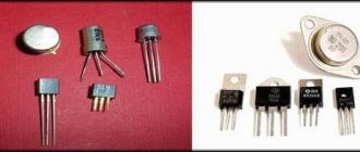
Basic types of transistors
There are two main types of transistors - bipolar and field-effect. In the first case, the output current is created with the participation of carriers of both signs (holes and electrons), and in the second case - only one. Testing the transistor with a multimeter will help determine the malfunction of each of them.
Bipolar transistors are essentially semiconductor devices. They are equipped with three pins and two pn junctions. The operating principle of these devices involves the use of positive and negative charges - holes and electrons. Flowing currents are controlled using a specially dedicated control current. These devices are widely used in electronic and radio engineering circuits.
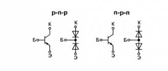
Bipolar transistors consist of three-layer semiconductors of two types - “p-p-p” and “p-p-p”. In addition, the design has two pn junctions. The semiconductor layers are connected to external terminals through non-rectifying semiconductor contacts. The middle layer is considered the base, which is connected to the corresponding pin. Two layers located at the edges are also connected to the outputs - the emitter and collector. In electrical circuits, an arrow is used to indicate the emitter, indicating the direction of current flowing through the transistor.
In different types of transistors, holes and electrons - carriers of electricity - can have their own functions. The most common type is p-p-p due to the best parameters and technical characteristics. The leading role in such devices is played by electrons, which perform the main tasks of ensuring all electrical processes. They are approximately 2-3 times more mobile than holes, and therefore have increased activity. Qualitative improvements in devices also occur due to the collector junction area, which is significantly larger than the emitter junction area.
Each bipolar transistor has two pn junctions. When testing a transistor with a multimeter, this allows you to check the performance of the devices by monitoring the resistance values of the transitions when direct and reverse voltages are connected to them. For normal operation of the p-p-p-device, a positive voltage is applied to the collector, under the influence of which the base junction opens. After the base current occurs, the collector current appears. When a negative voltage occurs in the base, the transistor closes and the current flow stops.
The base junction in pnp devices opens when exposed to negative collector voltage. Positive voltage causes the transistor to turn off. All the necessary collector characteristics at the output can be obtained by smoothly changing the current and voltage values. This allows you to effectively test the bipolar transistor with a tester.
There are electronic devices in which all processes are controlled by the action of an electric field directed perpendicular to the current. These devices are called field-effect or unipolar transistors. The main elements are three contacts - source, drain and gate. The design of the field-effect transistor is complemented by a conductive layer that acts as a channel through which electric current flows.
These devices are represented by modifications of the “p” or “p”-channel type. Channels can be located vertically or horizontally, and their configuration can be volumetric or near-surface. The latter option is also divided into inversion layers containing enriched and depleted ones. The formation of all channels occurs under the influence of an external electric field. Devices with near-surface channels have a metal-dielectric-semiconductor structure, which is why they are called MOS transistors.
Hand made probe assembly
A homemade device (probe) will immediately determine the serviceability of a transistor of any type. Let us present the simplest effective scheme.
What you will need (only 3 working components):
- in addition 2 elements. The LED is connected to the secondary winding through a resistor. 100 Ohm, its power is not important, as is the polarity of the first element, since a variable value appears at the output.
- base – any small down-trans. (from a switching power supply, from a household light bulb, small household appliances). Our primaries have 24 rounds with a middle tap; secondary – 15;
There is also a slot for inserting parts to be controlled according to the pinout. For bipolar straight wire types (KT 814... 818, etc.) the base passes through a resistor to one of the intermediate contacts, which (coupler) is connected to the "+" power supply. We connect the outlet to the power supply “-”, assembly. – free exit of primary organs. If the conductivity of the part is reversed, simply change the "+" and "-". Likewise with field workers, the main thing is to follow the pinout. If the indicator lights up after turning on the power, the product is working.
The probe is powered by 3.7–6 V; A lead-acid or lithium-ion battery will do.
Checking a bipolar transistor with a multimeter
This is the most common component, for example the KT315, KT361 series, etc.
There will be no problems with testing this type; it is enough to imagine the pn junction as a diode. Then the pnp and npn structures will look like two counter- or reverse-connected diodes with a midpoint (see Fig. 3).
Figure 3. “Diode analogues” of pnp and npn junctions
We connect the probes to the multimeter, the black one to “COM” (this will be a minus), and the red one to the “VΩmA” socket (plus). We turn on the testing device, switch it to the dialing or resistance measurement mode (it is enough to set the limit to 2 kOhm), and begin testing. Let's start with pnp conductivity:
- We attach the black probe to terminal “B”, and the red one (from the “VΩmA” socket) to leg “E”. We look at the multimeter readings; it should display the value of the junction resistance. The normal range is 0.6 kOhm to 1.3 kOhm.
- In the same way we take measurements between terminals “B” and “K”. The readings should be in the same range.
If during the first and/or second measurement the multimeter displays minimum resistance, then there is a breakdown in the transition(s) and the part requires replacement.
- We reverse the polarity (red and black probe) and repeat the measurements. If the electronic component is working properly, the resistance will be displayed, tending to the minimum value. If the reading is “1” (the measured value exceeds the capabilities of the device), an internal break in the circuit can be stated, therefore, the radio element will need to be replaced.
Testing a reverse conduction device follows the same principle, with a slight modification:
- We connect the red probe to leg “B” and check the resistance with the black probe (touching terminals “K” and “E” in turn), it should be minimal.
- We change the polarity and repeat the measurements, the multimeter will show a resistance in the range of 0.6-1.3 kOhm.
Deviations from these values indicate a component failure.
Methods for checking TRZ
Method No. 1: with direct connection
A simple algorithm for checking any types of TRZ and diodes:
1.Connect the red (plus) probe to the base of the transistor being tested, and the black (minus) probe to the collector terminal.
Photo 4 - Connecting probes
2. The red probe is left in place, and the black one is connected to the emitter terminal.
Photo 5 - The junction conducts current. This method allows you to check the transition when you turn it on directly.
Method No. 2: when turned back on
To make sure it works, it is better to double-check it when connecting it back: the pn junction will not be able to conduct current, and the number 1 should be displayed on the multimeter screen - this will mean that the junction resistance is very high and there is no way to pass current.
To check the transition in reverse inclusion you need:
1. Change the polarity of the probes to the transistor output, that is, connect the negative one to the base, and the positive one to the collector.
Photo 6 - Value 1 on the multimeter: PN junction does not pass current during reverse connection
We tested the TRZ in two ways and made sure it worked.
Transistors are of two types:
- NPN;
- PNP.
The table shows examples of types of transistors that differ in functionality.
| Model | Description |
| Control of the resistance of a current-carrying channel using a transverse electric field. |
| In welding machines and in devices where there are heavy loads. |
| In televisions for generating current in the horizontal scanning system, generating high voltage on an amplifier, kinescope, and powering circuits. |
| Always open when voltage is applied to the gate. |
| Equipped with three electrodes and one junction. Used in pulse and measuring instruments. There is a section with negative differential resistance. |
Variety TRZ
| Model | Description |
| Features an insulated shutter. Used in industry and electrical appliances. |
| Used for motors, relays, regulators. |
| Due to the housing, SMD technology (SMD) is used for surface mounting. |
| High power, isolated shutter. |
| The operating principle is to change the electric field in a semiconductor. |
Comparison table of popular transistor models
| Model | Description |
| Silicic. Low-frequency and high-voltage, used in various power supplies (switching), for mobile gadgets and chargers. |
| Silicon bipolar. Used in various electronic devices. They are inexpensive, but belong to the low-power class. |
| Silicon bipolar. Used in various electronic devices. Cheap. |
| Bipolar. Used in TVs and radios. |
| Bipolar. High power and isolated shutter. Used in welding machines and engines. |
| Silicic. Low-frequency and high-voltage, used in various power supplies (switching), for mobile gadgets and chargers. |
| Silicon and high voltage. Used in various electronic devices. |
| Silicon bipolar. Used in various electronic devices. It is inexpensive and belongs to the powerful class. |
| Silicon and high voltage. Used in various electronic devices. |
| Silicon bipolar transistor. Used in electronic devices. Cheap and powerful. |
| Silicon bipolar. Cheap and powerful. |
| Silicon bipolar. They belong to the powerful class. |
| Used in circuits with amplifiers and switches. |
| Silicic. Low-frequency and high-voltage, used in various power supplies (switching), for mobile gadgets and chargers. |
| Silicic. Low-frequency and high-voltage, used in power supplies (switching), for mobile gadgets and chargers. |
| Bipolar. High power, isolated shutter. Used in welding machines and engines. |
| High current gain. Used in TVs and radios. |
| Needed to control the resistance of the current-carrying channel using a transverse electric field. |
| To control the resistance of a current-carrying channel using a transverse electric field. |
| For generating current in horizontal scanning systems and generating high voltage. |