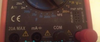
Transistors, along with capacitors and resistors, are one of the main elements on electrical device boards and are almost always present in circuit design. These parts control current from a small impulse, so incorrect selection, any breakdown leads to a significant disruption in the functionality of the devices, and often because of this they burn out. We will describe ways to check a transistor, and this will need to be done when analyzing faults in electrical appliances and when selecting spare parts for assemblies.
What is a transistor
Transistors replaced electric lamps and made it possible to reduce the number of relays and switches in devices. These are semiconductor triodes - radio-electronic components made from semiconductors; they have 3 terminals as standard.
Transistors are designed to control current, that is, the main power factor of electrical circuits; it is its shock (not voltage) that poses a danger to humans.
The element is capable of controlling extremely high values in output circuits when applying a weak input signal. Transistors boost, generate, switch, and convert electrical signals; they are the basis of microelectronics and electrical devices.
Varieties based on operating principle:
- bipolar transistor made of 2 types of conductors, the basis of its operation is the interaction of adjacent pn sections on the crystal. They consist of an emitter/collector/base (hereinafter, we will abbreviate these terms): the latter receives a weak current, causing a modification of the resistance (hereinafter referred to as “resistance”) in the line consisting of the first 2 elements. Thus, the flowing quantity changes, the side of its unidirectionality (npn or pnp) is determined by the characteristics of the transitions (sections) in accordance with the polarity of the connection (reverse, forward). Control is carried out by modulating the current on the base/emitter segment, the output of the latter is always common for control and output signals;
- field. There is only one type of conductor - a narrow channel subject to the electric field of a separate gate passage. Control is based on modulating the number of volts between it and the source. And between the latter and the drain an electric current flows (2 working contacts). The value has a strength depending on the signals generated between the gate (control contact) and one of the specified parts. There are products with a pn control section (working contacts are connected to a p- or n-semiconductor) or with separate gates.
Field workers have polarity options; low voltage is required for control; due to their efficiency, they are installed in radio circuits with low-power power supplies. Bipolar variants are activated by currents. In analog assemblies, the latter (BT, BJT) prevail, in digital (processors, computers) - the former. There are also hybrids - IGBTs, used in power circuits.
Advantages and disadvantages of bipolar transistors
The advantages of bipolar transistors in comparison with analogues include:
- control of electrical charges;
- reliability in operation;
- resistance to frequency interference;
- low noise characteristics;
The disadvantages include:
- has a low input resistance, due to which the signal amplification characteristics deteriorate;
- severe sensitivity to static charges;
- the connection diagram assumes the presence of 2 power supplies;
- At high temperatures the transistor may be damaged.
Checking bipolar types
Below is a diagram for checking npn, pnp transistors with a tester, after which we will describe the procedure point by point.
The bipolar transistor is equipped with pn lines - conventionally, these are diodes, or rather, 2 of them located oppositely, the point of their intersection is the “base”.
One conditional diode is designed with base/collector contacts, the other with base/emitter contacts. For analysis, just look at the contrast. (directly and back) of the indicated areas: if there are no problems there, then the part is without flaws.
Do-it-yourself testing without soldering a bipolar pnp, npn transistor involves testing 3 combinations of legs:
pnp option
Structures (types) are shown by the arrow emitting. section: pnp/npn (to/from the base). Let's start by checking the first option. We open the PNP part by applying negative voltage to the base. On the multimeter, we set the selector to measure Ohms to o; it is also possible to set it to “continuity”.
The vein “−” (black) is on the base leg. Plus (red) - alternately to collect., emitter. If the areas are not damaged, they will display about 500–1200 Ohms.
Next we will describe how to ring the reverse resistance: “+” - to the base, “−” - to the call. and emits. High resistance should be displayed. on both pn sites. We now have “1”, that is, for the frame set to “2000” the value exceeds 2000. This means that there are 2 transitions without breaks, the product is in good working order.
Similarly, as described, you can test the transistor for serviceability without removing it from the circuit. Less commonly, there are assemblies where substantial shunting is applied to the transitions, for example, with resistors. Then, if too low resistance is displayed, the part will need to be desoldered.
npn structure
Npn elements are checked in the same way, only the “+” probe goes to the base from the tester.
Symptoms of a problem
If the resistance (direct and reverse) of one of the sections (pn) tends to infinity, that is, at o and above on the display “1”, which means that this section has a break, the transistor is unusable. If “0” means the product is also flawed, the area is broken. Direct cont. there should be 500–1200 ohms.
First steps
The first thing to do is determine the characteristics of the transistor and its type. Regular marking helps with this. Type it into your browser and you will find a technical description that contains information about the type, pinout, etc. Another name for technical documentation from the manufacturer is datasheet, so don’t be alarmed if you come across such a word. And don’t worry, if the datasheet is in another language, you will be able to recognize the necessary symbols. As a last resort, an online translator can help you.
After it becomes clear what kind of element is in front of you, you need to remove it. We will tell you below how to test a transistor with a multimeter without desoldering it and whether it can be done.
Transistors are divided into several types, so the process of testing each of them is slightly different. We will consider each option.
Where is the base, collector, emitter
We determine the base leg (the mode is the same - “2000 Ohms”): “+” of the tester we touch the left contact, “−” - the rest one by one.
Legs left/middle “1”, left/right - 816 Ohms. So far this is not very informative. Use the “+” probe for the middle contact, “−” for the rest.
The result is similar. The next stage: “+” on the right leg, “−” on the middle and then on the left.
We get “1” each, that is, resistance. is the same in these areas and it goes to infinity. It turns out that we measured the inverse of this value on both pn segments. So the base is the right leg. But the complete procedure for checking serviceability involves finding a call. and emits. direct resistance measurements We touch the base output with a minus, and the rest with a “+”.
The leg on the left is 816 Ohm, this is emitter, the middle leg is 807 Ohm, this is collector, the value there is always lower.
The result is this:
- available type - pnp;
- base on the right, em. - left; coll. - in the middle.
Checking field effect transistors
Continuity, without desoldering, of the field-effect transistor, similar to that for an unmounted copy. Field workers are sensitive to static - before the event it is removed by grounding. It is enough to touch the spare part with one hand and the heating batteries with the other. To check field-effect transistors, their pinout is determined before the procedure.
Markers by which you can determine the conclusions (not always available, especially on domestic products): S - source, D - drain, G - gate. They also look at the technical documentation; the data is available on the Internet.
How to test a field effect transistor:
- We remove the static.
- We set the mode for semiconductors (“dialing”).
- We insert the red “+” wire and the black “–” wire into the corresponding sockets of the multimeter.
- “+” to the source, “−” to the drain. Operating condition: 0.5–0.7 V.
- We change the probes. If the numbers go to infinity, the transistor is working.
- “+” to the gate, “−” to the source, opening occurs. We do not disconnect the last wire, the first one goes to the drain. A working copy will show 0–800 mV. We change the polarity of the wires - the values should not change.
- We close: “−” - to the gate, “+” - to the source.
The serviceability of the field switch is determined by its opening/closing (whether this is observed at all) by applying a low voltage from the tester. The input capacitance in the element is large, and it takes a certain time to discharge. This is important, since first the multimeter opens with a small voltage (item 4), and then measurements must be taken within a short period (items 6, 7).
The procedure for checking a field-effect transistor of type p is the same as for n, only you need to connect the red probe to “−” and the black probe to “+”, that is, change the polarity.
Composite transistors
To test a composite transistor, you need to turn it on. It is convenient to use a pointer tester installed for resistance analysis. (1000 or 2000 Ohm). For the npn type: probe “+” - for the collector, negative - for the emitter. For pnp it's the other way around. The arrow will be indestructible (at the beginning of the “infinity” section), and in the digital multimeter “1”. If you moisten your finger and make a short circuit, touch it to the leg of the base and the commutator, the arrow will move, as the part will open slightly. The serviceability of the transistor is confirmed.
Features of the device
For composite transistors, the gradual decrease in voltage along the conductor at the base-emitter junction is twice the standard. The level of voltage reduction across an open transistor is approximately equal to the voltage drop that the diode has.
According to this indicator, a composite transistor is similar to a step-down transformer. But relative to the characteristics of the transformer, the Darlington transistor has much greater power gain. Such transistors can operate switches with a frequency of up to 25 Hz.
The system for the industrial production of composite transistors is set up in such a way that the module is fully equipped and equipped with an emitter resistor.
IGBT test
IGBTs have an insulated gate and are 3-electrode power semiconductor elements. Here, 2 transients are connected in cascade. in 1 structure: field and bipolar (control and power channels).
You can analyze the transistor on the board and soldered using a similar method. The tester is used to analyze semiconductors (“continuity”, diode icon) or resistance. 2000 Ohm. Then the resistance is measured. in the emitter/gate section straight and back. This way we will identify the short circuit, if there is one. Next, the red wire is connected to the emitter, the black wire is briefly touched to the shutter. The latter is charged with negative voltage, the transistor remains closed.
The next point is to confirm functionality. The gate-emitter input section is charged with positive voltage: at the same time, the red conductor is briefly touched to the gate, and the black conductor is briefly touched to the emitter.
Next, we check the transition point between the calls. and emitter: red wire to the first, black to the other. If a slight drop in value of 0.5–1.5 V is displayed and the value lasts for several seconds. stable, then input. The capacity is intact, the transistor is working.
Testing powerful high-voltage transistors has a peculiarity. If the multimeter voltage is not enough to open the IGBT, then 9–15 V sources are used to charge it at the output, for example, a 9 V Krona battery.
How to test a unijunction transistor
Let's take KT117 as an example; a fragment from its specification is shown in Figure 8.
Fig 8. KT117, graphical representation and equivalent circuit
The element is checked as follows:
We switch the multimeter to continuity mode and check the resistance between legs “B1” and “B2”; if it is insignificant, we can state a breakdown.
Digital transistors
A digital transistor is a special type, there are specifics on how to check it correctly.
The components of digital transistors are resistors. (R1 and 2), their rating is the same (10, 22, 47 kOhm) or mixed, different. Externally, the product has a normal appearance, but when ringing, significant differences arise.
A convenient device for checking transistors is an ampere-voltmeter, you can also take a multimeter. When the direction is direct, when the segment is open, resistance will appear on the tester. approximately comparable to the base resist. R1. When changing the polarity of the probes, the base/emitter point. closed, current flows through resistors connected in series. R1 (10 kOhm) and 2 (22 kOhm), the display will show the sum of their resistances, in our example 32 kOhm.
Base-issue segment. (VD2) is shunted by resistor R2. The resistance there should be approximately 10 times lower than R2, and when the polarity of the AVOmeter is changed, it should be infinitely greater.
What parameters are taken into account when choosing a bipolar transistor?
- The material from which it is made is gallium arsenide or silicon.
- Frequency. It can be ultra-high (more than 300 MHz), high (30-300 MHz), medium (3-30 MHz), low (less than 3 MHz).
- Maximum power dissipation.
Sources
- https://ElectroInfo.net/poluprovodniki/chto-takoe-bipoljarnyj-tranzistor.html
- https://principraboty.ru/bipolyarnyy-tranzistor-princip-raboty-dlya-chaynikov/
- https://radio-samodel.ru/tranzistor.html
- https://popayaem.ru/bipolyarnyj-tranzistor-princip-raboty-dlya-chajnikov.html
- https://vsbot.ru/lektronika/chto-takoe-bipolyarnyi-tranzistor-i-kak-ego-proverit.html
- https://microtechnics.ru/sxemy-vklyucheniya-bipolyarnogo-tranzistora/
- https://pue8.ru/silovaya-elektronika/832-kharakteristiki-i-parametry-tranzistorov.html
- https://www.RadioElementy.ru/articles/bipolyarnye-tranzistory/
How do you like the article?
Thyristor testing
Let's also consider how to ring thyristors; they are in many ways similar to the parts under consideration. There are 3 pn segments, but the mode does not change after the control signal - this is the difference. The structures run alternately like stripes on a zebra crossing. Thyristor is open until the flow value drops “to the holding current”. Such details allow you to create economical circuits.
The multimeter is set to 2000 ohms. To open the thyristor being tested, the black wire goes to the cathode, the red wire goes to the anode. The part opens with both a “+” and “−” charge. In two cases, resistance must be less than "1". The part is open if the value of the control pulse exceeds the holding frame; if it is less, the key is closed.
Assembling a makeshift sampler
A homemade device (probe) will allow you to instantly determine the serviceability of a transistor of any type. Let us present an elementary effective scheme.
What you will need (3 working components in total):
- the basis is any small downshift. (from pulsed power supplies, ballast for housekeeper light bulbs, small electrical appliances). Our primary has 24 turns with a middle tap; secondary - 15;
- further, 2 elements. The LED is connected to the secondary through a resistor. 100 Ohm, its power is not important, as is the polarity of the first element, since a variable value appears at the output.
There is also a slot for inserting parts to be tested according to the pinout. For bipolar straight-through types (KT 814...818 and so on), the base goes through a resist. to one of the transform contacts, medium output. which (tap) is connected to the “+” power supply. Emit. connect to “−” power supply, collection. - to have a free day off. primary If the conductivity of the part is reversed, then simply change “+” and “−”. Similarly with field workers, the main thing is to maintain the pinout. If light appears after power is applied, then the product is working.
The probe is powered from 3.7–6 V; a lead or lithium-ion battery is suitable.
Bipolar transistor connection circuits
A bipolar transistor has three terminals: emitter, collector and base. A signal comes to two of them, and from the other two it is removed, because one of them is common for entry and exit. So, which electrode is connected to the common bus, so is the connection diagram: with a common emitter (CE), a common base (CB) or a common collector (CC).
a) The connection circuit for a bipolar transistor with an OE is used most often in practice. In the above circuit, the input signal is supplied between the base and emitter through a decoupling capacitor Cp in order to cut off the DC voltage from the previous stage and not affect the power supply to the next stage. The amplified alternating voltage is removed from the collector and common terminal. This connection circuit provides both current and voltage gain. Such a connection will have a high output resistance (up to tens of kiloohms and depends on the value of Rk), but a low input resistance (500-1000 Ohms).
b) The following diagram shows switching on with OK. The bipolar transistor in this case works as a current amplifier and the voltage values at the input and output are almost the same. A feature of this connection is the high input resistance (from 10 kOhm to 500 kOhm), which provides good matching with the signal source stage. Also, the phase of the output voltage coincides with the phase of the input (there is no “flip” of the output signal, as in a circuit with an OE). Therefore, such a connection is called an emitter follower. But its output resistance is low, which greatly depends on the load resistance Re.
c) In the circuit with OB, we “ground” the base to the common wire through the capacitor Sat. In this case, the transistor only amplifies voltage, but there is no current amplification. Its input resistance is small (tens of ohms), and such a connection is used mainly in generators.
Connection diagram with a common base.
This circuit is very good when using high frequency signals. In principle, this is what switching on the transistor is used for in the first place. Very big disadvantages are the low input resistance and, of course, the lack of current amplification. See for yourself, at the input we have the emitter current I_e, at the output I_k.
I_e = I_k + I_b
That is, the emitter current is greater than the collector current by a small amount of the base current. This means that there is not just no current gain, moreover, the output current is slightly less than the input current. Although, on the other hand, this circuit has a fairly large voltage transfer coefficient. These are the advantages and disadvantages, let’s continue...
Connection diagram for a bipolar transistor with a common collector
This is what the wiring diagram for a bipolar transistor with a common collector looks like. Doesn't remind you of anything? If we look at the circuit from a slightly different angle, we will recognize our old friend here - the emitter follower. There was almost a whole article about it (here it is), so we have already covered everything related to this scheme. Meanwhile, we are waiting for the most commonly used circuit - with a common emitter.
Connection circuit for a bipolar transistor with a common emitter.
This circuit has earned popularity for its amplifying properties. Of all the circuits, it gives the greatest gain in current and voltage; accordingly, the increase in signal power is also large. The disadvantage of the circuit is that the amplification properties are strongly influenced by increasing temperature and signal frequency.
We got acquainted with all the circuits, now let’s take a closer look at the last (but not the least important) amplifier circuit based on a bipolar transistor (with a common emitter). First, let's depict it a little differently:
There is one minus here - the grounded emitter. When the transistor is turned on in this way, there are nonlinear distortions at the output, which, of course, must be combated. Nonlinearity occurs due to the influence of the input voltage on the emitter-base junction voltage. Indeed, there is nothing “extra” in the emitter circuit; the entire input voltage turns out to be applied precisely to the base-emitter junction. To cope with this phenomenon, we add a resistor to the emitter circuit. So we will receive negative feedback.
We recommend reading: NE555 circuit: universal practical projects
What is this?
In short, the principle of negative feedback is that some part of the output voltage is transferred to the input and subtracted from the input signal. Naturally, this leads to a decrease in the gain, since the input of the transistor, due to the influence of feedback, will receive a lower voltage value than in the absence of feedback.
Nevertheless, negative feedback is very useful for us. Let's see how it will help reduce the influence of the input voltage on the voltage between the base and emitter.
So, even if there is no feedback, an increase in the input signal by 0.5 V leads to the same increase in U_{be}. Everything is clear here. Now let’s add feedback! And in the same way we increase the input voltage by 0.5 V. Following this, U_{be} increases, which leads to an increase in the emitter current. And an increase in I_e leads to an increase in the voltage across the feedback resistor. It would seem, what's wrong with this? But this voltage is subtracted from the input! Look what happened:
The input voltage has increased - the emitter current has increased - the voltage across the negative feedback resistor has increased - the input voltage has decreased (due to the subtraction of U_{os}) - the voltage U_{be} has decreased.
That is, negative feedback prevents the base-emitter voltage from changing when the input signal changes. As a result, our amplifier circuit with a common emitter was supplemented with a resistor in the emitter circuit:
There is another problem with our amplifier. If a negative voltage value appears at the input, the transistor will immediately close (the base voltage will become less than the emitter voltage and the base-emitter diode will close), and nothing will happen at the output. This is somehow not very good... Therefore, it is necessary to create an offset. This can be done using a divisor as follows:
We got such a beauty. If resistors R_1 and R_2 are equal, then the voltage on each of them will be equal to 6V (12V / 2). Thus, in the absence of a signal at the input, the base potential will be +6V. If a negative value, for example -4V, comes to the input, then the base potential will be equal to +2V, that is, the value is positive and does not interfere with the normal operation of the transistor.
How else can we improve our circuit... Let us know what signal we will amplify, that is, we know its parameters, in particular the frequency. It would be great if there was nothing at the input except the useful amplified signal. How to ensure this? Of course, with the help of a high-pass filter! Let's add a capacitor, which in combination with a bias resistor forms a high-pass filter:
This is how the circuit, in which there was almost nothing except the transistor itself, was overgrown with additional elements. Perhaps we’ll stop there; soon there will be an article devoted to the practical calculation of an amplifier based on a bipolar transistor. In it we will not only draw up a circuit diagram of the amplifier, but also calculate the ratings of all elements, and at the same time select a transistor suitable for our purposes. See you soon!
Input characteristics for a common emitter circuit.
Let us depict the characteristics of the already considered transistor KT603A (Fig. 1.60).
Now the Earley effect manifests itself in the fact that as the voltage uke increases, the characteristics shift to the right. The differential resistance is now determined by the expression rdif= (dube/dib) |ib– given, uke= const
Output characteristics for a common emitter circuit
Let us depict these characteristics for the KT603A transistor (Fig. 1.61).
Let us turn to the previously obtained expression ik=αst·ie+iko In accordance with Kirchhoff's first law ie=ic+ib and taking into account the previous expression we obtain ikαst· (ic+ib) +icо from where ik=αst/ (1 -αst) ·ib + 1 / (1 -αst) iko
Let us introduce the notation: βst ≡ αst / (1- αst )
The coefficient αst is called the static transfer coefficient of the base current. Its value is usually tens - hundreds (this is a dimensionless coefficient).
It is easy to see that 1 / (1 -αst) = βst + 1 Let us introduce the designation i′ko ≡ (βst + 1) ·iko As a result, we obtain iк= βst ·ib+i′ko This expression, to a first approximation, describes the output characteristics in the active region work without taking into account the slope of the characteristics.
To take into account the slope, the expression is written in the form ik= βst ·ib+i′ko +ukb· ( 1 /r′к), where r′к =duke/dik|uke – given, ib=const
To a first approximation, r′k = ( 1 / 1 + βst) · rk (resistance rk is defined above). The so-called differential base current transfer coefficient β is often used.
To increase the collector current ∆iк and base current ∆ib, we can write:
∆iк ≈ β ∆ iб
By definition β=diк/diб|iк – given, uke=const
For the KT603A transistor at t = 25°C β = 10...80.
The value of β depends on the operating mode of the transistor. Let us present a typical graph of the dependence of β on the emitter current (it is almost equal to the collector current) for ukb = 2 V (Fig. 1.62).
For normal operation of the transistor at direct current, in addition to the condition Pk < Pk max discussed above, the conditions ik must be met
For the KT603A transistor discussed above, ik max = 300 mA, uke max = 30 V (at t < 70 ° C).
Let us schematically depict on the output characteristics for a circuit with a common emitter the so-called safe operation area in which the specified conditions are met (Fig. 1.63).
It is usually acceptable to assume (with some error) that the output characteristics for a circuit with a common emitter are located on straight segments fan-shaped from one point on the voltage axis (Fig. 1.64).
The voltage Ue (this is a positive value) is called the Early voltage. For transistor KT603A Ue ~ 40 V.
Bottom line
Any transistor is checked with a multimeter. You need to find out the purpose of its legs (base/col./emitter, drain/source/gate). Next, set the tester to “continuity” or to the 2000 Ohm mark. Then analyze forward and reverse resistance. Based on the result, you can determine the performance of the transistor. You can also analyze the coefficient. amplification: the tester has a special socket and an hFE mark.

